IC Design
The final project for a class at Iowa State (EE330) was creating a schematic and layout for an IC circuit in Cadence.
Design Constraints:
-
Two control pins (A0 and A1) are used to decide the output of the device.
-
For AoA1 = 00, the circuit output performs as a non-inverting amplifier.
-
For AoA1 = 01, the circuit output performs as an inverting amplifier.
-
For AoA1 = 10, the circuit output performs as a digital potentiometer.
-
For AoA1 = 11, the circuit output performs as a DAC with a reference voltage of 1 volt.
-
Four control pins (C0, C1, C2, and C3) can vary the resistance of the potentiometer, the gain of both the inverting and - - non-inverting operational amplifier, and the output voltage of the DAC.
-
The potentiometer must have 16 taps with a difference of 500 ohms between each tap. The chip must have two inputs denoted as Vtop and Vbottom that can be set anywhere between -2.5 volts and 2.5 volts to change the VDD and VSS reference voltages for the potentiometer.
-
A digital potentiometer should be used to control the gain of the inverting and non-inverting operational amplifier.
-
The digital potentiometer and an operational amplifier configured as a unity gain buffer should be used to form the DAC.
-
The entire chip must have a VDD of 2.5 volts and VSS equal to -2.5 volts.
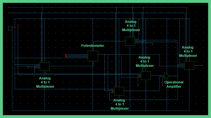
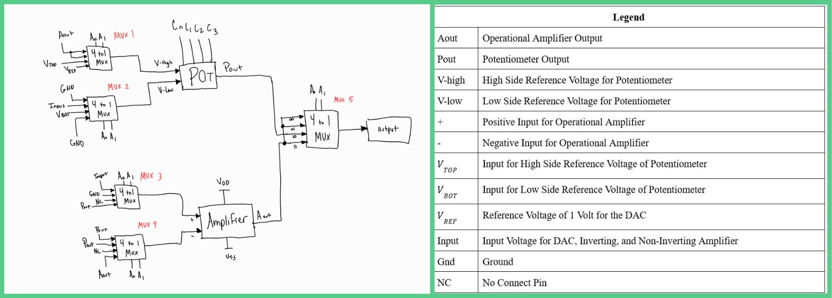 Block diagram for the high level design for the IC.
A potentiometer and an operational amplifier are used for many of the outputs, and no two outputs are used simultaneously, so we designed the circuit to have a single operational amplifier and potentiometer for all four functionalities. The inputs and outputs of the potentiometer and operational amplifier could be re-routed for the chosen functionality by adding 5 analog 4-to-1 multiplexers. The design chosen reduces the layout size by decreasing the number of components needed when compared to a design that uses individual potentiometers and amplifiers for the non-inverting, inverting, potentiometer, and DAC outputs. Analog multiplexers have a smaller layout than operational amplifiers and potentiometers, thus decreasing the total size of the IC even further. The tradeoff of this design is that the outputs cannot be used simeultaneously and components can not be invidually optimized for a specific output because all components must work for all outputs. These tradeoffs are not a problem though, because the IC fits within the design constraints.
Components:
2-4 Decoder:
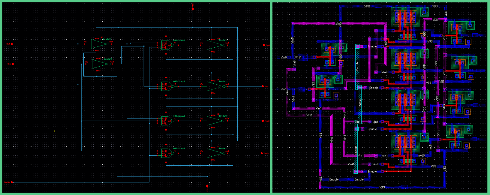 Schematic and layout for 2-4 decoder.
The 2-4 decoder is a stepping stone to implement the 4-16 decoder. The 2-4 decoder was made using 4, 3 input NAND gates and 6 NOT gates. The boolean expressions for a 2-4 decoder where “F” represents outputs and “in” represents inputs are:
F1 = ~in1 & ~in0
F2 = in1 & ~in0
F3 = ~in1 & in0
F3 = in1 & in0
The schematic shows this implementation. The NAND and NOT gates on the right of the scematic make up AND gates (NAND->NOT = AND) and the NOT gates on the left negate the inputs to the NAND gates where necessary to match the boolean expressions. The NAND gates are 3 input instead of 2 because this 2-4 decoder also has an enable pin.
4-16 Decoder:
 Schematic and layout for 4-16 decoder. Implemented using 5, 2-4 decoders made above.
Transmission Gate:
The transmission gate allows for bidirectional current flow which is necessary for AC signals. Transmission gates were implemented in the design of the analog 4-to-1 multiplexer and the potentiometer. A typical transmission gate is composed of a NMOS transistor, a PMOS transistor, and an inverter. The transmission gate made for this project has 3 NMOS transistors in parallel and 3 PMOS transistors in parallel. The parallel transistors were originally implemented on a misunderstanding. The potentiometer output was too small and we thought it was due to faults in the transmission gates implemented in the potentiometer. We later realized it was an issue with the way we had designed the resistor ladder in the potentiometer, but by that time the layouts for the transmission gate had already been made, so they were not changed due to time constraints. Under ideal circumstances, there would be a single PMOS and NMOS transistor for this project as it would reduce the number of transistors needed and the total size of the layout. On the other hand, parallel transistors could be beneficial depending on the application as it could allow for more current flow. The transmission gate designed for this project is composed of 5 pins, the gate (G), drain (D), source (S), VDD (vdd), and VSS (vss).
 Schematic and layout for the transmission gate.
Analog 4-to-1 Multiplexer:
The analog 4-to-1 multiplexer allows for switching between analog signals using digital logic. It is implemented using a 2-to-4 decoder and 4 transmission gates. 5 4-to-1 multiplexers are present in the final design.
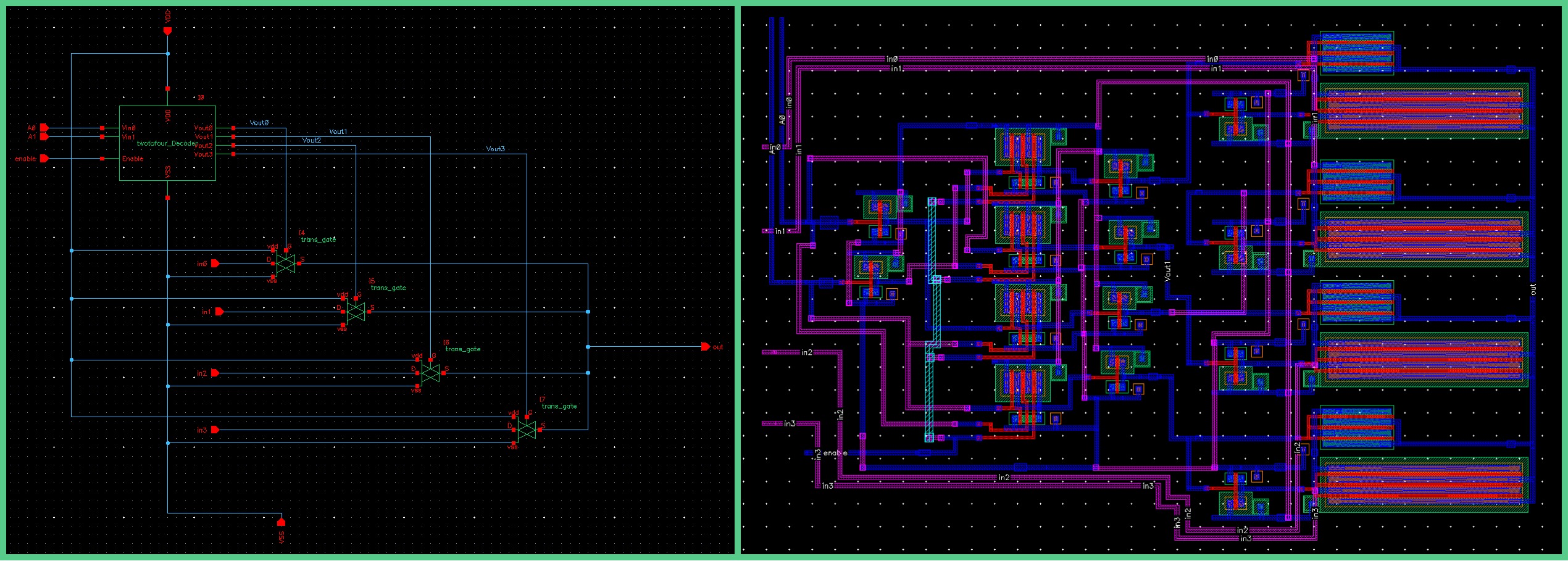 Schematic and layout for the analog 4-to-1 multiplexer. A 2-to-4 decoder with select pins A0 and A1 controls the voltage on 4 transmission gates. Depending on the values of A0 and A1, the output pin (labeled out) is connected to either in0, in1, in2, or in3.
Operational Amplifier: An operational amplifier can be used to magnify an input signal. In this project the operational amplifier is implemented in in two different configurations with the potentiometer to form a non-inverting and inverting output. The operational amplifier used in this project was a two stage externally compensated operational amplifier that makes use of a current mirror to amplify a signal similar in design to the one designed in the “Externally Compensated Op Amps” paper by Randy Gieger.
 Schematic and layout of the operational amplifier.
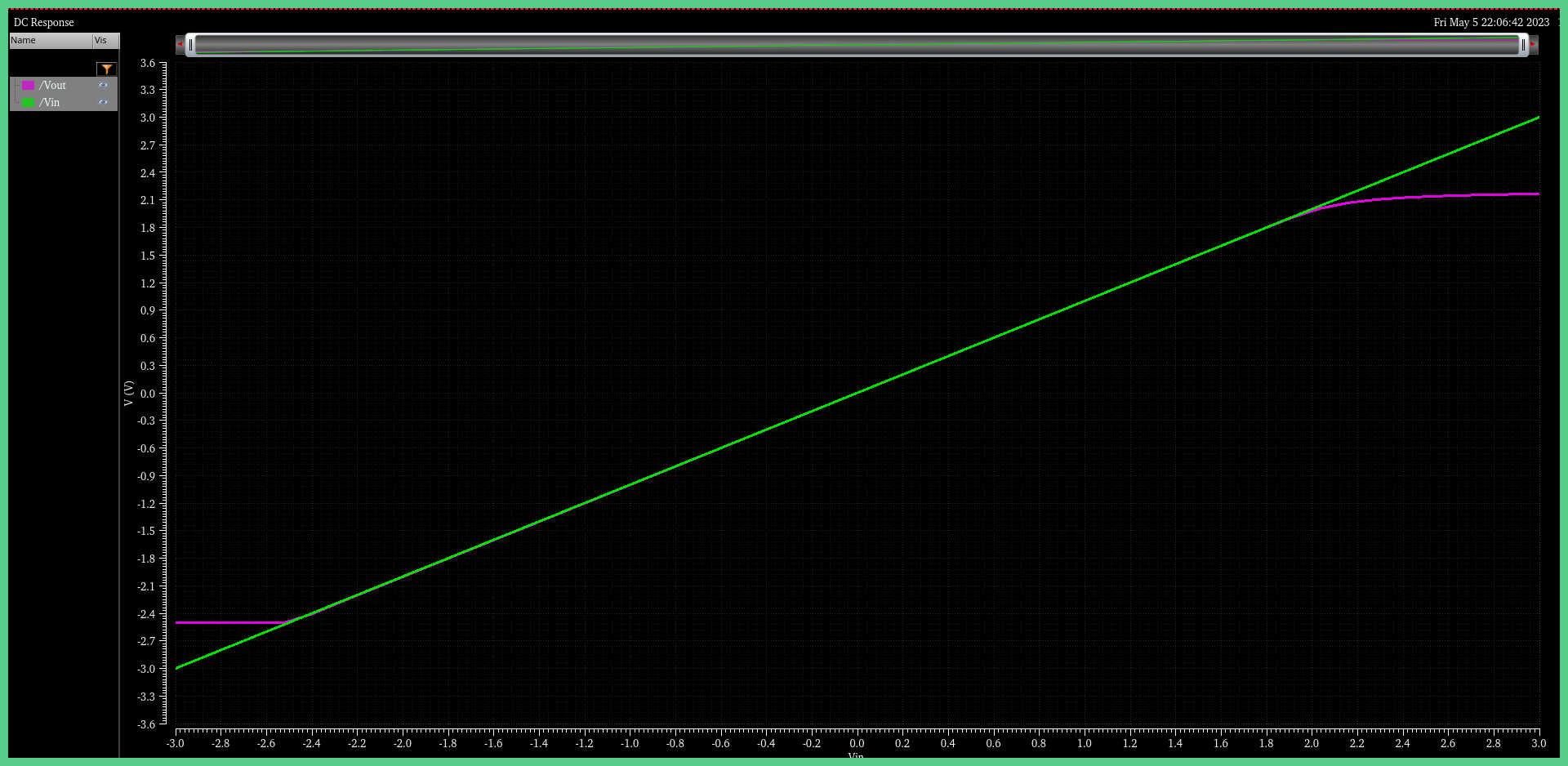 ICMR test for the operational amplifier. The test shows that the OP Amp operates in the linear region from about -2.4 V to +2.2V given a VDD and VSS signal of 2.5 V and -2.5 V.
An ICMR (input common-mode range) test determines the range of input voltages for which a device (in our case, the operational amplifier) maintains expected characteristics.
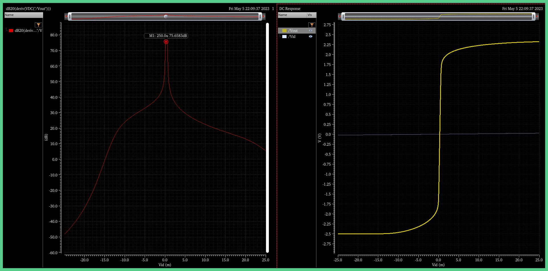 Results for the “Open Loop Gain” test. The image on the left shows an open loop gain of 75dB based on the V/V test on the right.
Potentiometer:
The potentiometer is an integral component within the overall circuit. The 4-to-16 decoder and the transmission gates are the only two sub circuits within the potentiometer. Together, they allow for a systematic switching/tapping of a resistor string via the C0, C1, C2, and C3 control inputs. This allows for a variable adjustment to the gain of the amplifier circuits. The potentiometer also functions as the Dac. By simply adjusting the A0 and A1 control inputs, we’re able to convert the potentiometer to have a static input of 1v. From there, we’re able to convert a digital signal from the C0, C1, C2, and C3 control inputs to analog.
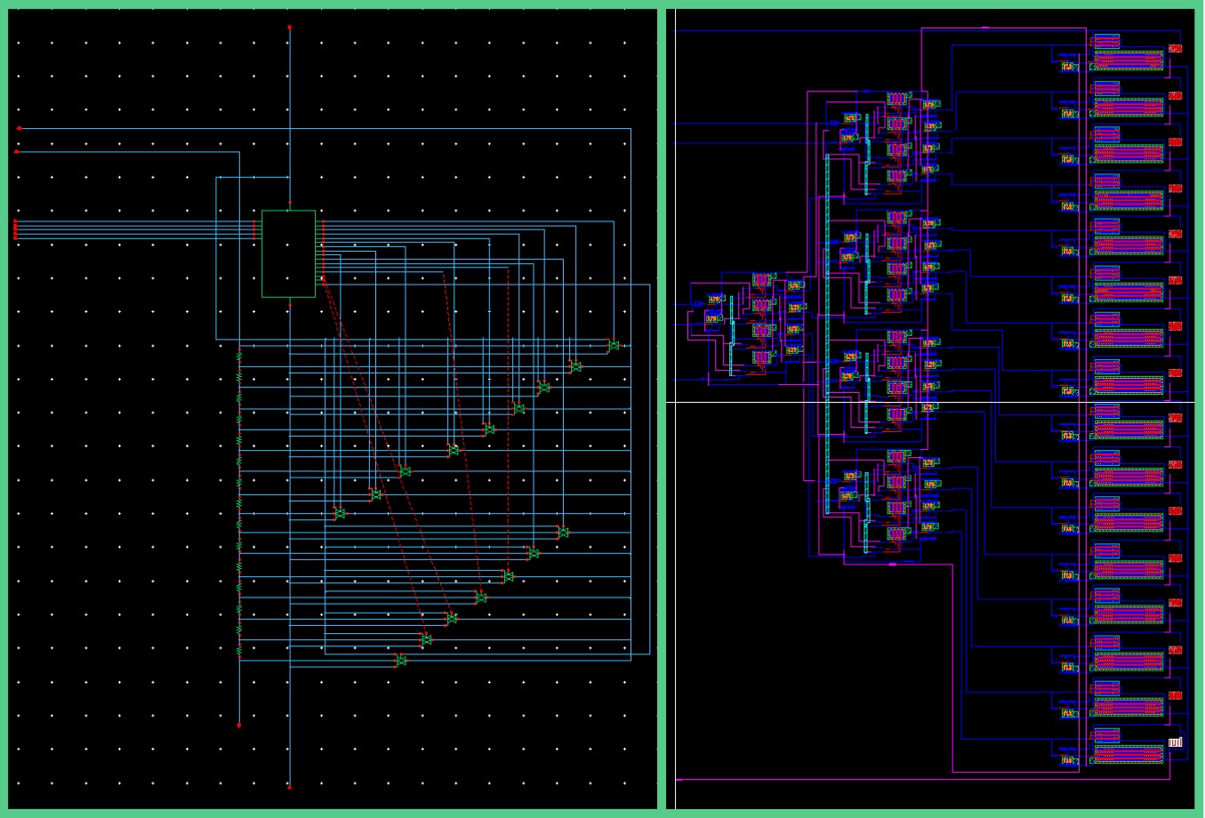 Schematic and layout for the potentiometer.
Final IC:
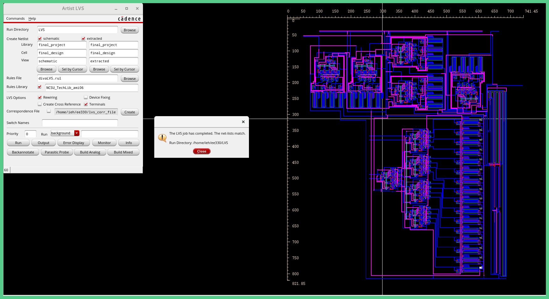 IC final layout
Outputs:
The chip has 4 outputs, a non-inverting op amp, an inverting op amp, a potentiometer and a DAC. The select pins C0, C1, C2, and C3 control the steps of the potentiometer and DAC, as well as the gain of the inverting and non-inverting amplifier. Which output is active is controlled by the select pins A0 A1.
Non-Inverting Operational Amplifier: A0A1 = 00
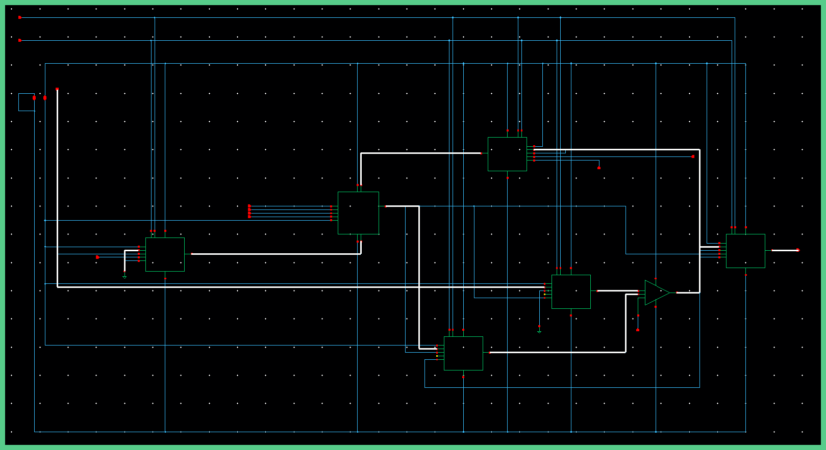 The highlighted traces represent which traces are active when A0 A1 = 00. The VDD, VSS, and enable, and C0 ,C1 ,C2 ,C3 traces would also have activity but were not highlighted as they may take away from the clarity of the image.
The non-inverting operational amplifier uses the potentiometer to form the negative feedback loop for the op amp. To form the negative feed-back loop, the output of the potentiometer connects to the negative input of the amplifier, the V_high of the potentiometer connects to the output of the amplifier, and the V_low side of the potentiometer connects to ground. The positive input of the operational amplifier is connected to the input signal provided by the user.
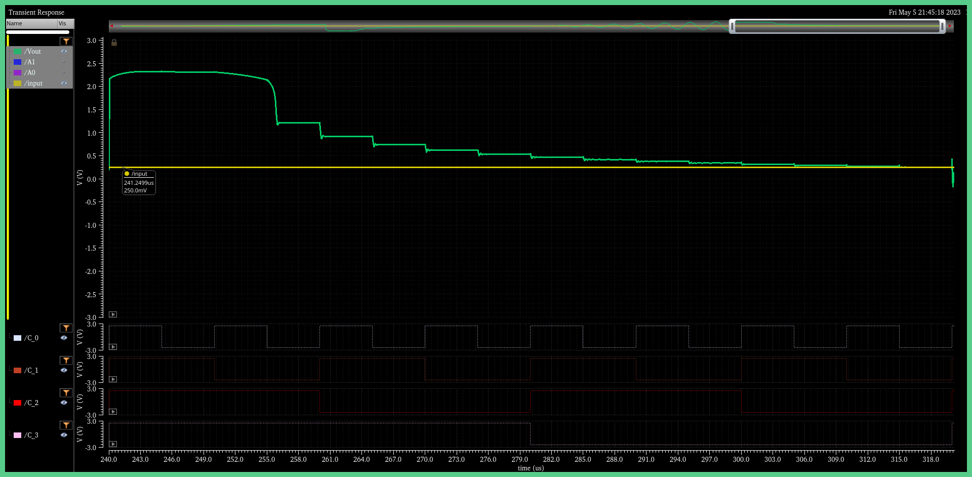 The positive DC response of the Non-Inverting Operational Amplifier. The signal being amplified is 250 mV. From the graph, it’s easy to see that amplified signal caps out rear the rail (Similar to the ICMR test).
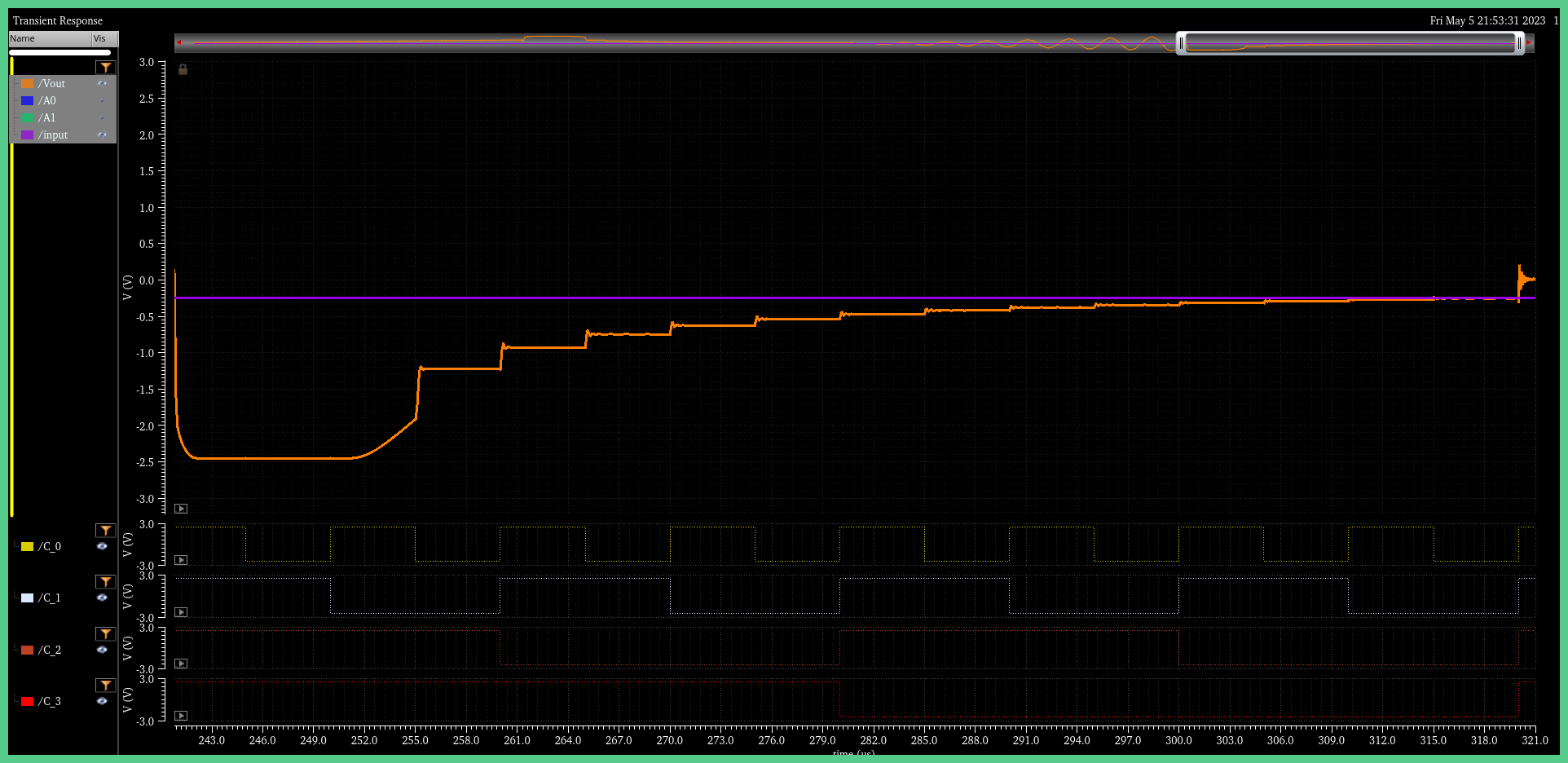 The positive DC response of the Non-Inverting Operational Amplifier. The signal being amplified is 250 mV. From the graph, it’s easy to see that amplified signal caps out rear the rail (Similar to the ICMR test).
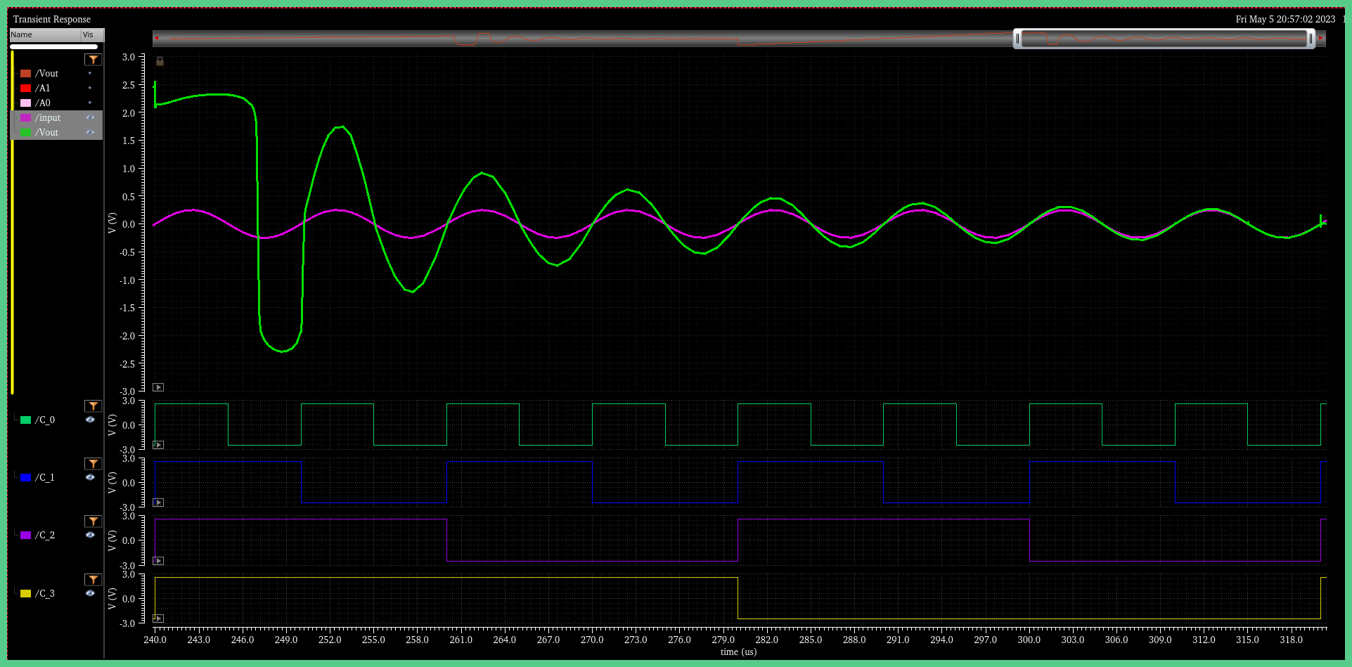 The AC response of the Non-Inverting Operational Amplifier. The signal being amplified is a 250mv 100k Hz AC signal. The amplified outputs caps out rear the negative rail (Similar to the ICMR test).
Inverting Operational Amplifier: A0A1 = 01
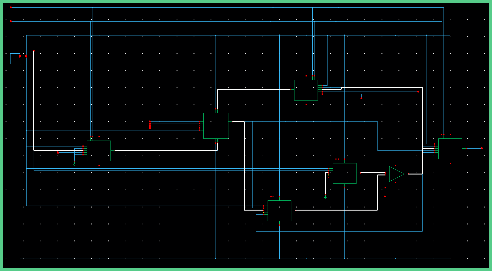 The highlighted traces represent which traces are active when A0 A1 = 01. The VDD, VSS, and enable, and C0 ,C1 ,C2 ,C3 traces would also have activity but were not highlighted as they may take away from the clarity of the image.
The potentiometer is used to form a negative feedback loop for the inverting op amp. The output of the potentiometer is connected to the negative input of the amplifier, the V_high of the potentiometer is connected to the output of the amplifier, and the V_low side of the potentiometer is connected to the input signal provided by the user. The positive input of the operational amplifier is connected to ground.
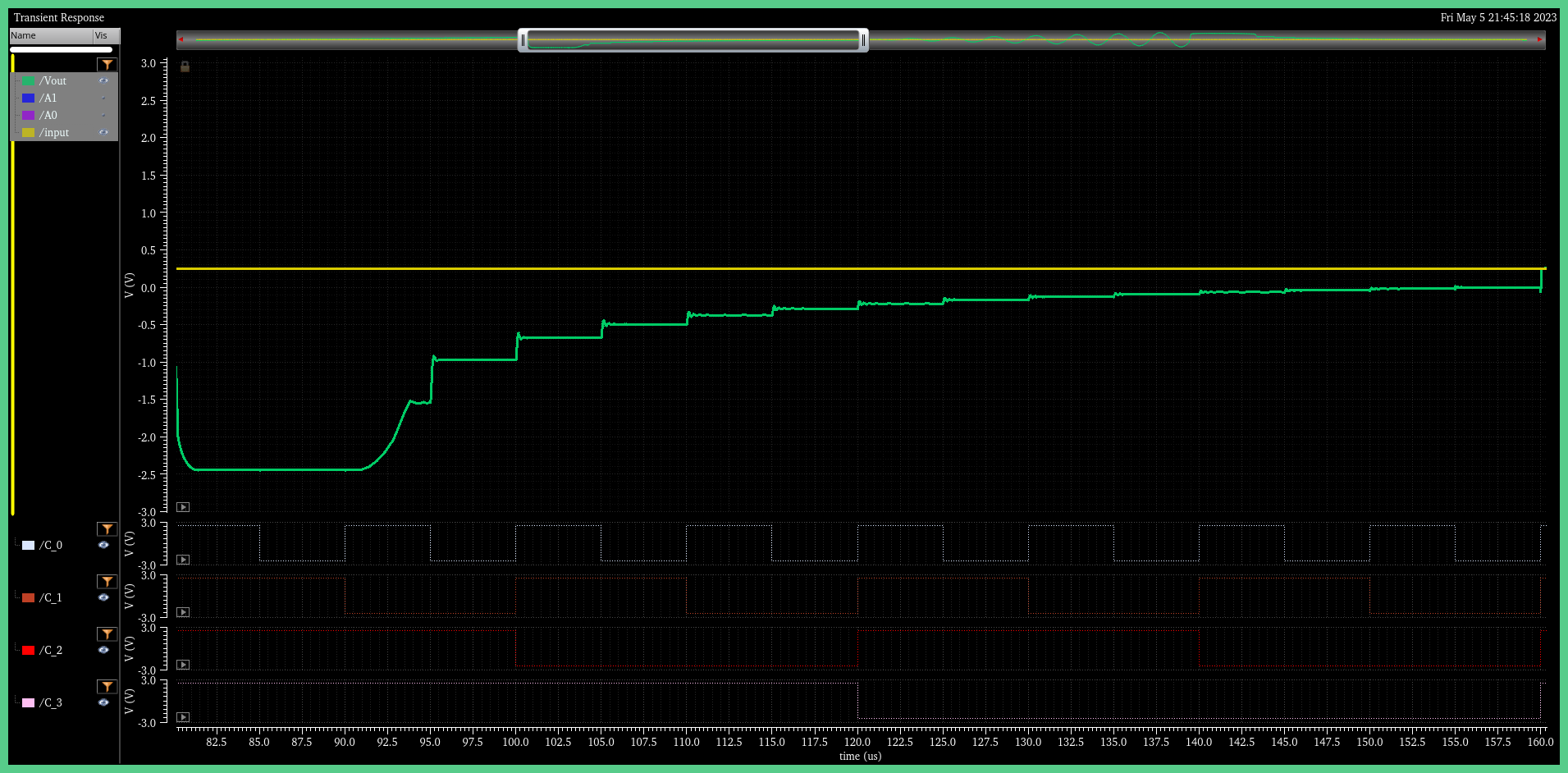 The positive DC response of the Inverting Operational Amplifier. The input signal is 250 mV. The amplified output signal caps out rear the rail.
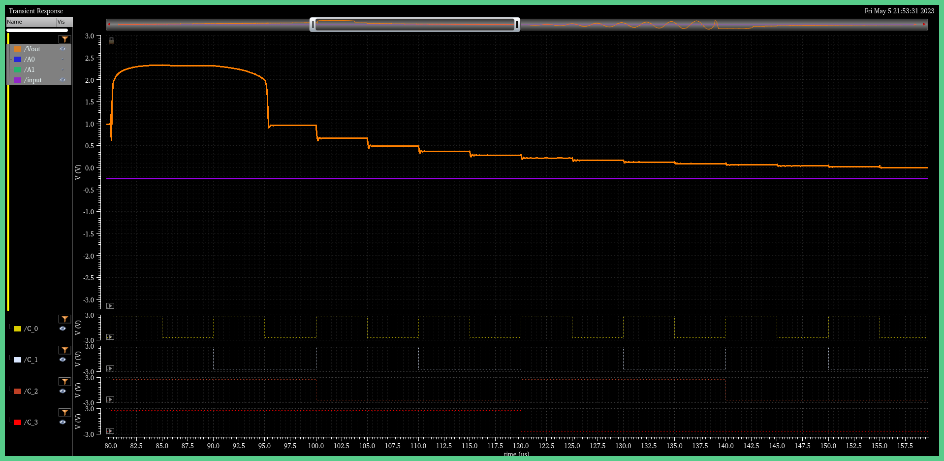 The negative DC response of the Inverting Operational Amplifier. The input signal is 250 mV.
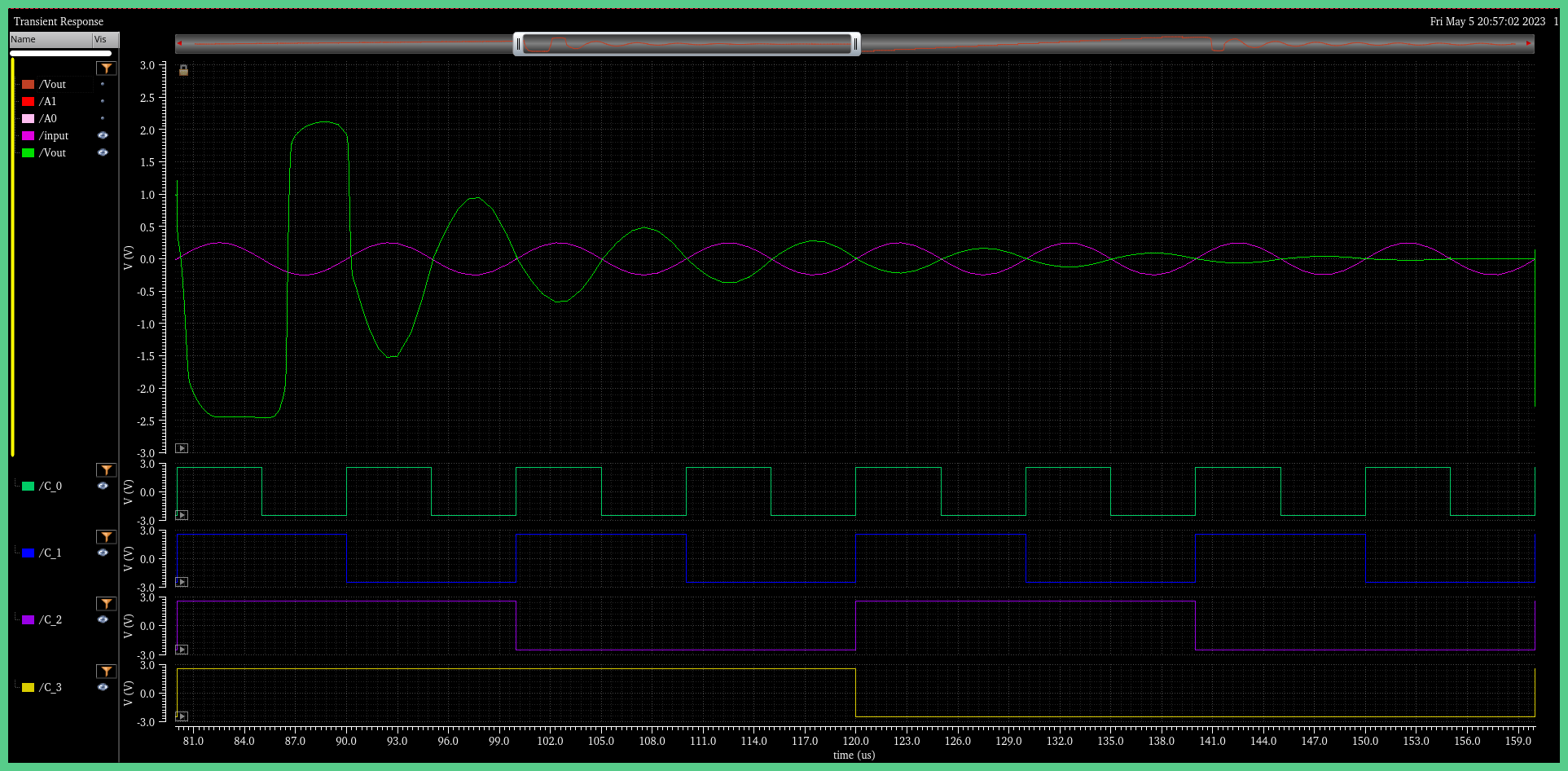 The AC response of the Inverting Operational Amplifier. The signal being amplified is a 250mv 100k Hz AC signal.
Potentiometer: A0A1 = 10
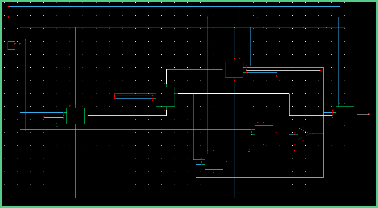 The highlighted traces represent which traces are active when A0 A1 = 10. The VDD, VSS, and enable, and C0 ,C1 ,C2 ,C3 traces would also have activity but were not highlighted as they may take away from the clarity of the image.
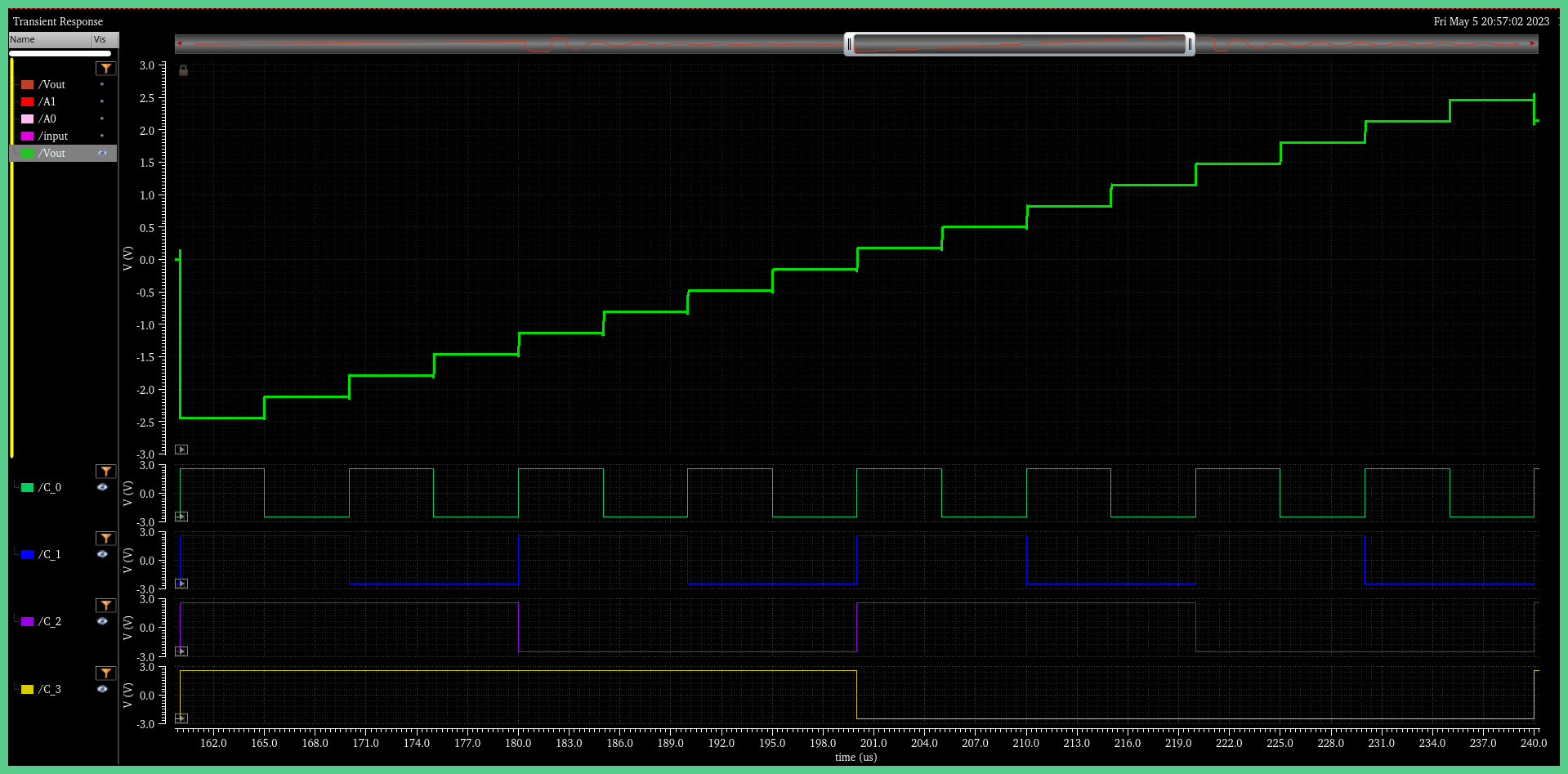 The DC response of the potentiometer. The input spans from -2.5V to 2.5V. There are 16 voltage steps because there are 4 control bits, C0, C1, C2, and C3.
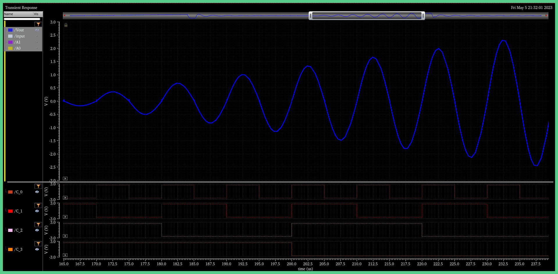 The AC response of the potentiometer. The input signal frequency is 100KHz and the amplitude spans from 0V to 2.5V.
DAC: A0A1 = 11
The DAC works by forming a series connection with the potentiometer and the operational amplifier in a unity gain configuration.The output of the potentiometer connects to the positive input of the amplifier and the output of the amplifier connects to the negative input of the amplifier.
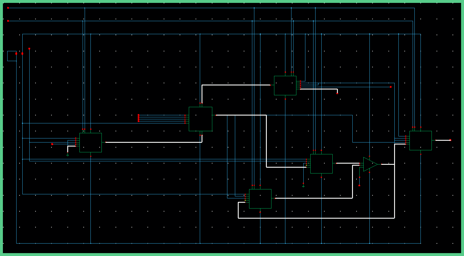 The highlighted traces represent which traces are active when A0 A1 = 11. The VDD, VSS, and enable, and C0 ,C1 ,C2 ,C3 traces would also have activity but were not highlighted as they may take away from the clarity of the image.
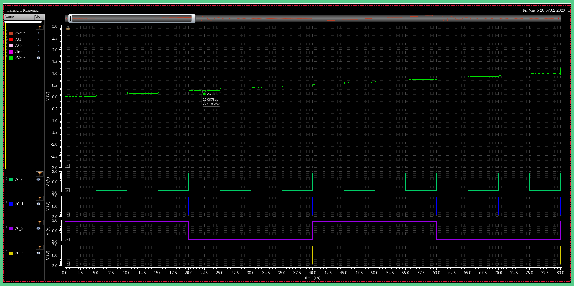 DAC response with DC voltage range from 0V to 1V.
Acknowledgements:
Jacob Steffens – partner for the project