MIPS Processor
Project Overview
A partner and I designed and tested a MIPS processor using VHDL for a college course (CPRE 381). There were three iterations of the design, a single cycle, a software pipelined, and a hardware piplined processor. After verifying the processor designs with Questasim, we compared performance metrics between the three designs by running MIPS assembly files on the VHDL hardware. We were able to ‘run’ the MIPS assembly files on the VHDL hardware by using software specifically designed for the class. All of the MIPS instructions that are possible on the hardware are in the table at the bottom of the page.
Single Cycle Processor
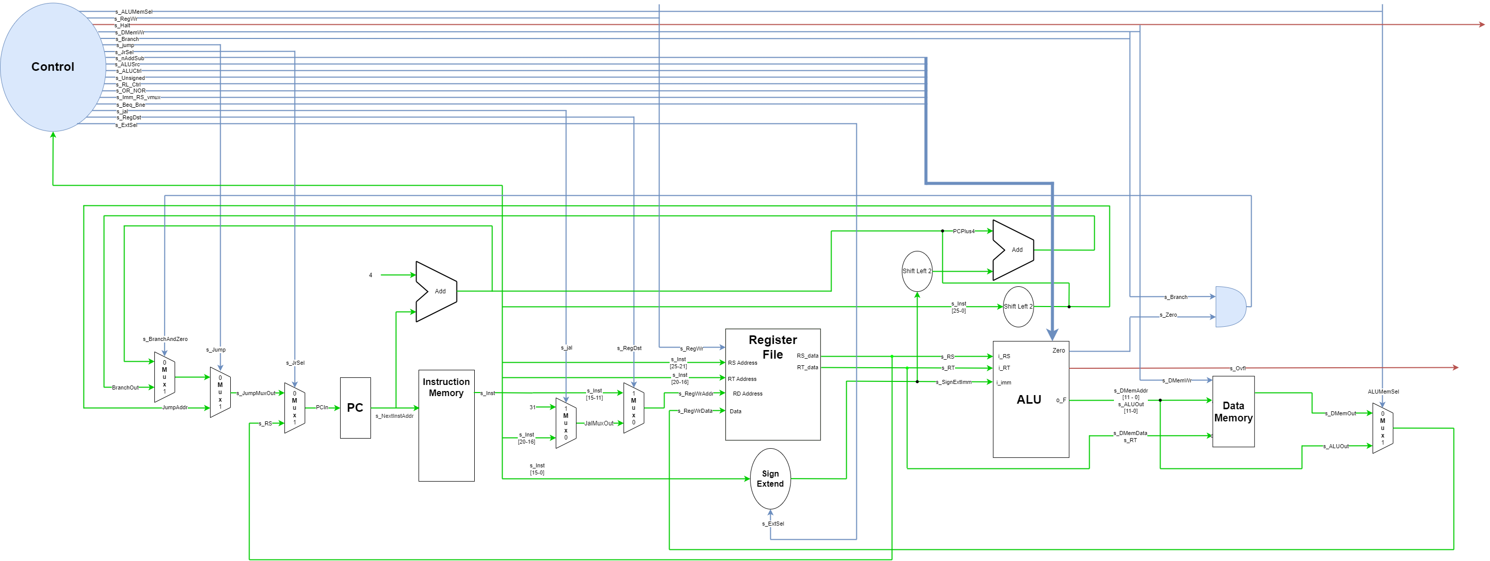
The single cycle processor was the first design we made. One MIPS instruction is executed each cycle of the clock. The blue lines represent control signals and the green lines represent data signals. The red lines (s_Halt and s_Ovfl) are required outputs of the processor so that the software simulating MIPS assembly files running on the VHDL processor will work.
Unit Test Example: Fetch Logic
This section will run through the VHDL implementation of the fetch logic for the single cycle processor, as well as the testbench and Questasim waveforms. Testbenches a Questasim simulations were done for all components in the design, but only this one is showed in the this page to keep this project report relativly short
Fetch Logic
The VHDL below is a structural implmentation of the fetch logic used in the single cycle processor. It starts by defining the entity, then defining the components that will be used for the fetch logic, defining intermediate signals that will connect the components, and finally instantiating and connecting the componets under the “begin” statement.
library IEEE;
use IEEE.std_logic_1164.all;

entity fetch_logic is
    port (
        CLK                     : in std_logic;
        RST                     : in std_logic;
        JumpSel                 : in std_logic;                     --If jump set to 1
        BranchAndOut            : in std_logic;                     -- If branch set to 1
        JrSel                   : in std_logic;
        SignExtImm              : in std_logic_vector(31 downto 0);
        Instruction             : in std_logic_vector(31 downto 0);
        RegRs                   : in std_logic_vector(31 downto 0);
        PCplus4                 : inout std_logic_vector(31 downto 0);
        PCOut                   : out std_logic_vector(31 downto 0)
    );
end entity;

architecture structural of fetch_logic is

--define components
    component FullAdder_N is
        generic(N : integer := 8);
        port(
            i0_N : in std_logic_vector(N-1 downto 0);
            i1_N : in std_logic_vector(N-1 downto 0);
            c_in : in std_logic;
            sum_N : out std_logic_vector(N-1 downto 0);
            c_out : out std_logic
        );
    end component;

    component mux2t1_N is
        generic(N : integer := 16);
        port(
        i_S          : in std_logic;
        i_D0         : in std_logic_vector(N-1 downto 0);
        i_D1         : in std_logic_vector(N-1 downto 0);
        o_O          : out std_logic_vector(N-1 downto 0));
    end component;

    component PCReg is
        generic(N : integer := 32);
        port(
        i_CLK        : in std_logic;                          -- Clock input
        i_RST        : in std_logic;                          -- Reset input
        i_WE         : in std_logic;                          -- Write enable input
        i_D          : in std_logic_vector(N-1 downto 0);     -- Data value input
        o_Q          : out std_logic_vector(N-1 downto 0));   -- Data value output
    end component;


    --define signals
    constant N32 : integer := 32;

    signal PCin                 : std_logic_vector(31 downto 0);
    signal jump_address         : std_logic_vector(31 downto 0);
    signal BranchAdd            : std_logic_vector(31 downto 0);
    signal BranchMuxOut         : std_logic_vector(31 downto 0);
    signal JumpMuxOut           : std_logic_vector(31 downto 0);
    signal PCOut_buffer         : std_logic_vector(31 downto 0);
    signal shiftedSignExtImm    : std_logic_vector(31 downto 0);


begin
    shiftedSignExtImm <= (SignExtImm(29 downto 0) & "00");
    -- (PCplus4(31 downto 28) : makes sure to stay in the section of memory for addresses
    -- (Instruction(25 downto 0) : address to jump to specified by instruction
    -- 00 : offsets the jump_address to be word alligned. 00 makes the address divisible by 4, which means word aligned.
    jump_address <= (PCplus4(31 downto 28) & (Instruction(25 downto 0) & "00"));

--define instances
    -- PC
    PC : PCReg
        generic MAP(N32)
        port MAP(
            i_CLK => CLK,
            i_RST => RST,
            i_WE  => '1',
            i_D => PCin,
            o_Q => PCOut_buffer
        );

    -- Adder0 = PC + 4
    Add4 : FullAdder_N
        generic MAP(N32)
        port MAP(
            i0_N => PCOut_buffer,
            i1_N => x"00000004",            --Add 4
            c_in => open,                   --No c_in
            sum_N => PCplus4,
            c_out => open                  --No c_out
        );

    -- Adder1
    BranchAdder : FullAdder_N
        generic MAP(N32)
        port MAP(
            i0_N => PCPlus4,
            i1_N => shiftedSignExtImm,
            c_in => open,               --not used
            sum_N => BranchAdd,
            c_out => open               --not used
        );

    -- MUX0
    BranchMux : mux2t1_N
        generic MAP(N32)
        port MAP(
            i_S => BranchAndOut,
            i_D0 => PCplus4,
            i_D1 => BranchAdd,
            o_O  => BranchMuxOut
        );

    -- MUX1
    JumpMux : mux2t1_N
        generic MAP(N32)
        port MAP(
            i_S => JumpSel,
            i_D0 => BranchMuxOut,
            i_D1 => jump_address,
            o_O => JumpMuxOut
        );

    -- MUX used for jr
    jrMuX : mux2t1_N
    generic MAP(N32)
    port MAP(
        i_S => JrSel,
        i_D0 => JumpMuxOut,
        i_D1 => RegRs,
        o_O => PCin
    );

    PCOut <= PCOut_buffer;
end architecture;
Fetch Logic Testbench
The VHDL below is the testbench that functions as a unit test for the fetch logic VHDL module shown above. It begins by defining the testbench entity, defining the components that will be used (in this case, just fetch_logic because it is being tested), defining signals that will connect to the ports of the fetch logic component, and finally writing test cases that check if the fetch logic component functions as expected. In this case, there is a test for a branch instruction, a jump instruction, and a non-branch and non-jump instrution.
library IEEE;
use IEEE.std_logic_1164.all;


entity tb_fetch_logic is
    generic(half_clk_period   : time := 5 ns);
end entity;

architecture tb of tb_fetch_logic is

    component fetch_logic is
        port (
            CLK                     : in std_logic;
            RST                     : in std_logic;
            JumpC                   : in std_logic;
            BranchAndOut            : in std_logic;
            SignExtImm              : in std_logic_vector(31 downto 0);
            Instruction             : in std_logic_vector(31 downto 0);
            PCOut                   : out std_logic_vector(31 downto 0)
        );
    end component;

    --reset and signal set above?
    signal s_CLK             : std_logic;
    signal s_RST             : std_logic;
    signal sJumpC           : std_logic;
    signal sBranchAndOut    : std_logic;
    signal sSignExtImm      : std_logic_vector(31 downto 0);
    signal sInstruction     : std_logic_vector(31 downto 0);
    signal sPCUout          : std_logic_vector(31 downto 0);
begin

    --instance
    DUT : fetch_logic
        port MAP(
            CLK => s_CLK,
            RST => s_RST,
            JumpC => sJumpC,
            BranchAndOut => sBranchAndOut,
            SignExtImm => sSignExtImm,
            Instruction => sInstruction,
            PCOut => sPCUout
        );

    --This first process is to setup the clock for the test bench
    tb_CLK: process
    begin
        s_CLK <= '1';         -- clock starts at 1
        wait for half_clk_period; -- after half a cycle
        s_CLK <= '0';         -- clock becomes a 0 (negative edge)
        wait for half_clk_period; -- after half a cycle, process begins evaluation again
    end process;


    tb_RST: process
    begin
        s_RST <= '0';
        wait for half_clk_period/2;
        s_RST <= '1';
        wait for half_clk_period*2;
        s_RST <= '0';
        wait;
    end process;

    --tests
    TEST_CASES : process
    begin
        wait for half_clk_period*3;
        -- case 1: next instruction in IMem
        sjumpC <= '0';
        sBranchAndOut <= '0';
        sSignExtImm <= x"00000000";   -- Does not matter
        sInstruction <= x"00000000";  -- Does not matter
        wait for half_clk_period*2;


        -- case 2: branch
        sjumpC <= '0';
        sBranchAndOut <= '1';
        sSignExtImm <= x"00000004";     --branch to location = (current location) + 4 + (4*4)  = (current location) + 20
        sInstruction <= x"00000000";    -- Does not matter
        wait for half_clk_period*2;


        -- case 3: jump
        --x0 + b1 + x1000023 + b00 = (PCplus4(31 downto 28) & (Instruction(25 downto 0) & "00"))
        -- b 0000 0100 0000 0000 0000 0000 1000 1100
        -- x0400008C
        sjumpC <= '1';
        sBranchAndOut <= '0';
        sSignExtImm <= x"00000000";    -- Does not matter
        sInstruction <= x"F1000023";    --bottom 26 bits taken for jump address. Expect: x0400008C
        wait for half_clk_period*2;
    wait;
    end process;

end architecture;
The waveform below is a simulation of the fetch logic testbench VHDL file. For the statements below, the “first clock cycle” refers to the second falling edge of the clock waveform. This is because of the “wait for half_clk_period*3;” in the testbench (I can’t remember why this was implemented at the time, and it may be unnecessary). The “second clock cycle” and “third clock cycle” are with reference to the “first clock cycle” starting at the second falling edge of the clock.
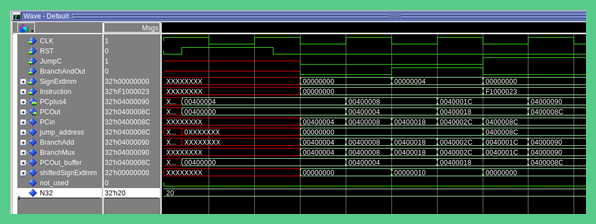
Test “next instruction”: The first clock cycle tests a case where the fetch logic would output PC+4. This occurs on a non-jump or non-branch instruction. In the waveform the PCplus4 signal matches the PCOut function which is the correct functionality.
Test Branch: The second clock cycle tests a branch case. The PCOut signal should the current branch location + 4 + (SignExtImm * 4) where SignExtImm = Sign Extended Immediate value. You multiply the SignExtImm by 4 because it is the same as shifting left by 2 which word alligns the SignExtImm value. The word allignment prevents you from jumping to a place in instruction memory that is not the start of an instruction. The SignExtImm is the offset to the address that the branch instruction will jump to, but it needs to be shifted by 2 (multiplied by 4) to be word alligned. The + 4 is to grab the next word/instruction in instruction memory after the branch. In the waveform the output is 0x00400018 = 0x00400004 + 4 + (0x00000004*4) where 0x00400004 is the previous instruction location in memory and 0x00000004 is the SignExtImm value.
Test Jump: The third clock cycle tests a jump case. The PCOut should equal to “PCplus4[31 - 28] & Instruction[25 - 0] & 00”. Given the instruction input of 0xF1000023 and the PCplsu4 value of 0x04000090 the output should be 0x0400008C, which it is.
Calculation for Test Jump case:
PCplus4[31 - 28] = 0b0000
Instruction[25 - 0] = 0b 01 0000 0000 0000 0000 0010 0011
PCplus4[31 - 28] & Instruction[25 - 0] & 00 = 0b 0000 0100 0000 0000 0000 0000 1000 1100
0b 0000 0100 0000 0000 0000 0000 1000 1100 = 0x0400008C
Software Scheduled Processor
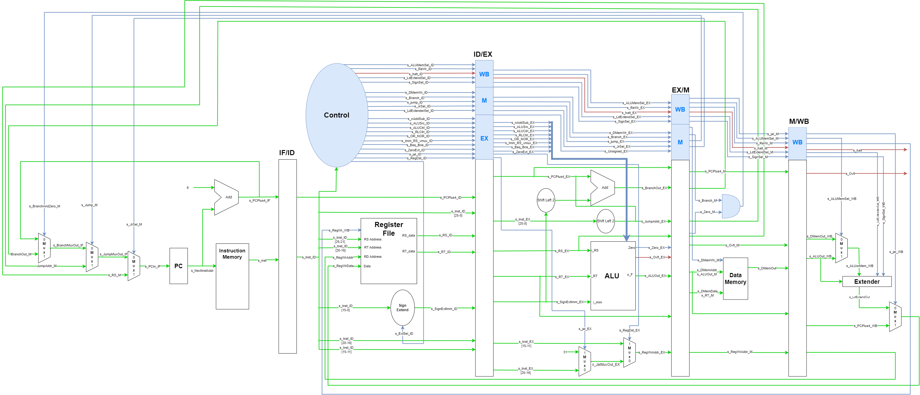
The difference between the single cycle and software scheduled pipelined processor is the addition of the pipeline registers, IF/ID, ID/EX, EX/M, M/WB. IF, ID, EX, M, WB are acronyms that stand for instruction fetch, instruction decode, execution, memory, and write back. The / in the names of the pipeline register mean that the register stores control and data signals between the two stages that make up the name of the register (for example, IF/ID means that the register stores values between the instruction fetch and instruction decode stage of the piplined processor).
Many signals must propagate through multiple stages before reaching their destination. To keep track of the signals, a naming convention was employed. The last two letters of most signals describe which stage they are in. If two signals in different stages have the same name (discluding the last two letters) then they represent the same signal in different parts of the pipeline (for example s_RS_ID and s_RS_EX represent the same signal, but one is in the instruciton decode stage and the other is in the execution stage). Signal names in the diagram are the same as the names used in the VHDL code.
| Acronym | Stage | Function |
|---|---|---|
| IF | Instruction Fetch | Fetches the MIPS assembly instruction from instruciton memory. 's_inst' is the data signal (in MIPS it is 32 bits long) in the IF stage that propagates the instruction into the IF/ID register |
| ID | Instruction Decode | Breaks down the s_inst signal to identify which MIPS instruction needs to be executed. s_inst is fed into the control component to determine the values of the control signals for the instruction. For some instructions parts of the s_inst signal are inputed into the register file as addresses to determine which registers will be outputed on the s_RS_ID and s_RT_ID signals |
| EX | Execution | Calculations involving the ALU are done here. This would include MIPS instructions that require addition, subtraction, bit shifting, or computational logic. If a MIPS instruction updates a register in the register file then the address is determined in this stage (the address is saved to the s_RegWrAddr_EX signal). If the MIPS instruction is a branch or jump insruction, then the branch or jump address is determined here. |
| M | Memory | Reads and writes to data memory are done here. Branch and jump instructions are executed here. |
| WB | Write Back | Data from the ALU or data memory is written back to the register file. The 'Extender' component shown in the software and hardware scheduled pipelined processors is used for assembly instrucitons load byte and load half-word which write back data different in size than a word (a word is 4 bytes in MIPS). |
Pipelining
Pipelining a processor decreases the length of the critical path (the path in the processor that takes the most time to execute) which allows the processor clock to run at a higher frequency. When running an instruction set on a pipelined processor, there is an initial ‘fill’ period, which is the amount of cycles required for all stages of the processor to have an instruction in progress. Our processor takes 5 cycles to fill since there are 5 stages, IF, ID, EX, M, and WB. After the initial fill period, each cycle of the processor will complete an instruction.
Data Hazards
Unlike a single cycle processor, pipelined processors have data hazards.
Data Hazard: Occurs when a register value is read or written by an instruction before it has been updated.
Example:
        ADD $8, $9, $10
        SUB $11, $12, $8
The ADD instruction is updating register 8 with the sum of registers 9 and 10. The next instruction, SUB is subtracting the value in register 12 from register 8 and putting the result in register 11. The issue is that the SUB instruciton will request the value of register 8 (happens in ID stage) before the results of the ADD instruction are written back to register 8 (happens in the WB stage).
In the software pipelined processor, hazards are avoided by adding NOP (no operation) instructions between MIPS instructions that cause data hazards. A NOP instruction does not perform any action, but stalls the processor long enough so that the register value is updated before it is used again. For the example given above, 3 NOPs would have to be added between the ADD and SUB instruction to avoid the hazard.

Assuming the example shown above, 3 NOP instructions are needed between the ADD and SUB instruction to avoid a data hazard. The ADD instruction must reach the WB stage before the SUB instruction reaches the ID stage so that register 8 is updated before it is used in the SUB instruction. Although not done here, 2 NOPs could be used instead of 3 if the processor was designed to have the WB execute in the first half of the clock cycle and the ID stage execute in the second half of the clock cycle.
Hardware Scheduled Processor
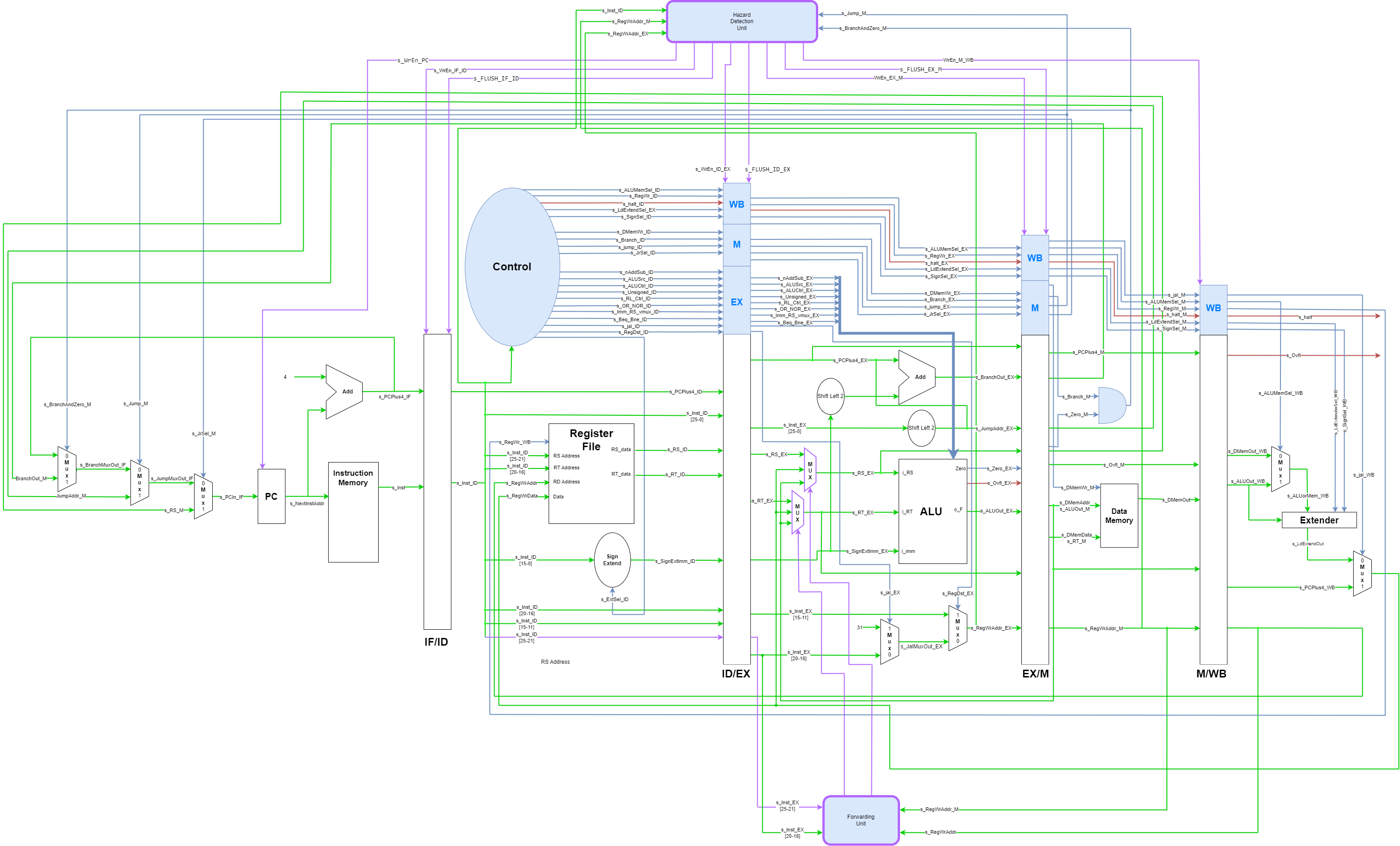
The forwarding unit and hazard detection unit (highlighted in purple) were added for the hardware scheduled piplined processor.
Hazard Detection
The hazard detection controls stalls and flushes for pipeline registers. The hazard detection unit allows the processor to avoid hazards without adding NOPs to the MIPS assembly instructions.
Stall: Holds values in a register by disabling the write enable for a pipeline register.
Flush: Sets all stored values in a pipelined register to 0 effectively creating a NOP.
The s_Inst_ID, s_RegWrAddr_EX, s_RegWrAddr_M, s_Jump_M, and s_BranchAndZero_M are input signals to the hazard detection unit shown in the Hardware Scheduled Processor diagram. Inside the hazard detection unit, the s_Inst_ID signal is decoded into the RS and RD addresses.

The RS and RD addresses are compared to the s_RegWrAddr_EX and s_RegWrAddr_M signals to see if the instruction in the ID stage is going to use a register that is currently in the pipeline and hasn’t yet reached the WB stage to update the register file. If a data hazard is detected, then the hazard detection unit stalls the PC (program counter), IF/ID pipeline register, and the ID/EX pipeline register until the Register File is updated in the WB stage.

You may notice in the above code there are only write enable signals for the PC (o_WrEn_PC), IF/ID pipeline register (o_WrEn_IF_ID), and ID/EX pipeline register (o_WrEn_ID_EX). To avoid data hazards, write enable control is only required on these 3 components, but we still need flush signals for the IF/ID, ID/EX, and EX/M pipeline registers. Besides the s_Stall_Data signal the write enable signals are also controlled by the s_FLUSH_ctrl signal. The write enable for the ID/EX pipeline register is also controlled by the s_FLUSH_Data signal. The s_FLUSH_Data and s_FLUSH_ctrl signals main purpose is to control the flush signals for IF/ID, ID/EX, and EX/M pipeline registers. The s_FLUSH_Data and s_FLUSH_ctrl signals control the write enable signals because the write enable signals have to equal 1 in order for the flush signal to affect the pipeline registers. The logic for s_FLUSH_Data, s_FLUSH_ctrl, and the flush signals are shown in the next image.
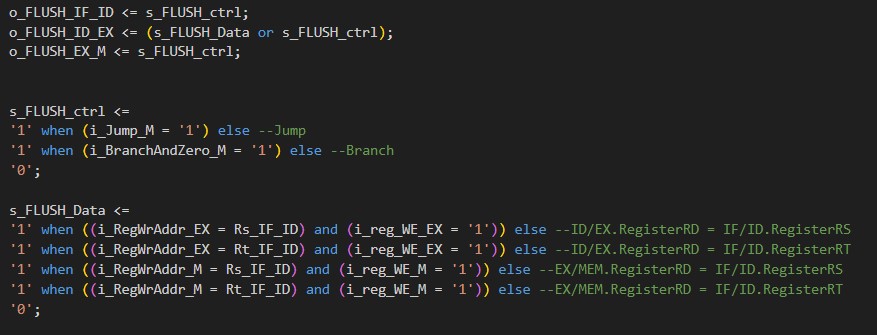
The o_FLUSH_IF_ID, o_FLUSH_ID_EX, and the o_FLUSH_EX_M signals are the flush signals for the IF/ID, ID/EX, and EX/M pipeline registers. The s_FLUSH_ctrl signal is used to flush the IF/ID, ID/EX, and EX/M pipeline registers when a branch or jump instruction is executed in the memory stage of the hardware pipelined processor. The s_FLUSH_Data signal flushes the ID/EX pipeline register for all hazards besides the jump and branch hazards. The flush caused by the s_FLUSH_Data on the ID/EX pipeline register acts as a NOP to prevent the processor from outputting garabge data from the instruction in the ID register that has a data dependency on the instruction in either the EX or M stage.
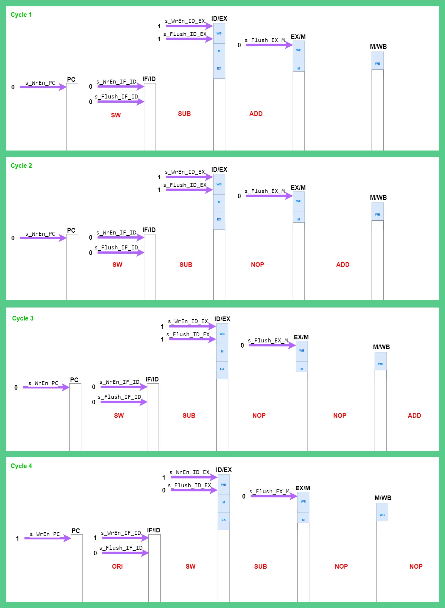 The diagram above shows 4 clock cycles where the SUB instruction has a data dependency on the ADD instruction. When the s_Flush_ID_EX signal is 1, it sets all values in the ID/EX register to 0, and creates a NOP instruction on the next clock cycle. Cycle 2 shows the first NOP instruction created by the flush signal in the EX stage. While the ID/EX register is flushed, the PC and IF/ID register are stalled to hold the values for the next instructions until the ADD instruction reaches the WB stage. Once the ADD instruction reaches the WB stage, the write enable signals for the ID/IF register and PC are set to 1, which disables the stalls and allows the instructions after the ADD instruction to flow through the pipeline (cycle 4).
Forwarding
Fowarding was not implemented in the VHDL code, but it is shown in the hardware scheduled processor diagram. Forwarding can improve the performance of the processor by removing the need for NOPs in the cases of a data dependency hazards. Instead of waiting for the leading instruction in a data dependent hazard to reach the WB stage to write back to the register file, the value that will be written to the register file (called s_DMemAddr and ALUOut_M in the M stage of the diagram) is sent back to the EX stage. Just like the hazard detection unit, the processor determines if it needs to forward by comparing the RS and RD addresses (s_Inst_EX [25-21] and s_Inst_EX[20-16]) with s_RegWrAddr_EX and s_RegWrAddr_M signals to see if they are the same.
Performance Comparison
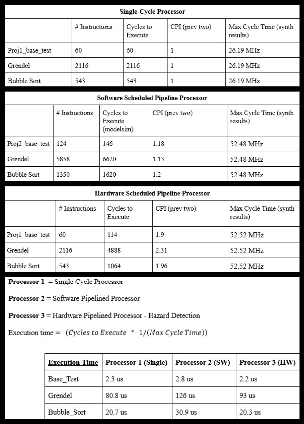
Performance between processors was compared using three MIPS assembly instruction sets. The ‘base_test’ assembly program would run every MIPS assembly instruction once. The grendel assembly program was a complicated instruction set given by our instructor that had many jumps and branches. The bubble_sort test was an assembly file my partner and I made that runs the bubble sort algorithm for an array specified at the top of the program. (The bubble sort algorithm orders an array from lowest number to highest number by swapping two adjacent entries if the right most entry is greater than the left most entry. The algorithm repeatedly runs through the array until no more swaps occur.)
| Instruction | Description |
|---|---|
| add | Adds two registers and stores the result in a register (with overflow) |
| addu | Adds two registers and stores the result in a register (without overflow) |
| addi | Adds an immediate value to a register and stores the result in a register (with overflow) |
| addiu | Adds an immediate value to a register and stores the result in a register (without overflow) |
| sub | Subtracts the second register from the first and stores the result in a register (with overflow) |
| subu | Subtracts the second register from the first and stores the result in a register (without overflow) |
| and | Performs a bitwise AND on two registers and stores the result in a register |
| andi | Performs a bitwise AND on a register and an immediate value, storing the result in a register |
| or | Performs a bitwise OR on two registers and stores the result in a register |
| ori | Performs a bitwise OR on a register and an immediate value, storing the result in a register |
| xor | Performs a bitwise XOR on two registers and stores the result in a register |
| xori | Performs a bitwise XOR on a register and an immediate value, storing the result in a register |
| nor | Performs a bitwise NOR on two registers and stores the result in a register |
| sll | Shifts a register value left by a specified number of bits (logical shift left) |
| srl | Shifts a register value right by a specified number of bits (logical shift right) |
| sra | Shifts a register value right by a specified number of bits (arithmetic shift right) |
| sllv | Shifts a register value left by a variable number of bits (logical shift left) |
| srlv | Shifts a register value right by a variable number of bits (logical shift right) |
| srav | Shifts a register value right by a variable number of bits (arithmetic shift right) |
| slt | Sets a register to 1 if the first register is less than the second (signed) |
| sltu | Sets a register to 1 if the first register is less than the second (unsigned) |
| slti | Sets a register to 1 if the register is less than the immediate value (signed) |
| sltiu | Sets a register to 1 if the register is less than the immediate value (unsigned) |
| beq | Branches to a specified address if two registers are equal |
| bne | Branches to a specified address if two registers are not equal |
| j | Jumps to a specified address |
| jal | Jumps to a specified address and links (stores the return address in $ra) |
| jr | Jumps to the address contained in a register |
| lw | Loads a word from memory into a register |
| lh | Loads a half-word from memory into a register (sign-extended) |
| lhu | Loads a half-word from memory into a register (zero-extended) |
| lb | Loads a byte from memory into a register (sign-extended) |
| lbu | Loads a byte from memory into a register (zero-extended) |
| lui | Loads an upper immediate value into a register |
| sw | Stores a word from a register to memory |
Acknowledgements
Tori Kittleson – My partner for the project. She developed the ALU, Extender, parts of the Control, the pipelined registers, and the extender unit which was used for instructions that were not word sized (4 bytes) such as lb and lh.