Distributed Sniffer Nodes for Batteryless Sensor Nodes
Project Overview
For senior design I worked with a team of 4 undergraduate students, 2 graduate students, and 1 professor who was also our client. The graduate students and professor were developing batteryless sensor nodes (referred to as BOBs throughout the project). During the senior design project the BOB was still in development, but the research team’s end goal for the BOB was a batteryless device that could collect sensor data in a variety of applications depending on the configuration and types of sensors attached to the BOB. The researchers also wanted communication between multiple BOBs forming a ‘BOB network’ that could send collected data back to a computer system for processing. Our goal as a senior design team was to develop a “sniffer” node which is a device that monitors and simulates sensory data for the BOB nodes. The sniffer is a test device and will not be part of the final BOB network. The goal of the sniffer is to provide a test setting for the BOB and verify the BOBs functionality.
Deliverable: Design and build a device called a “sniffer” that will monitor and verify the functionality of both a single batteryless sensor node (BOB node) and a network of BOB nodes.
Project Terms
- BOB = term used for the batteryless sensor node.
- Sniffer = device that monitors a single BOB node. 2 CC1352 radio chips are used for a 1 sniffer
- Faux BOB = a simulated BOB on a CC1352 radio chip.
- Primary = CC1352 radio chip on the sniffer that receives data from a BOB via a Sub 1GHz radio signal. Sends recieved data from the BOB to the relay via 3-wire SPI.
- Relay = CC1352 radio chip on the sniffer that receieves BOB data from the primary via 3-wire SPI. Sends recieved data from the Primary to the sink via 2.4GHz radio signal.
- Sink = Device that collects all the data from the sniffer nodes via 2.4GHz signal. It processes some of the data then passes it on to a computer system. It is also a programmed CC1352 radio chip.
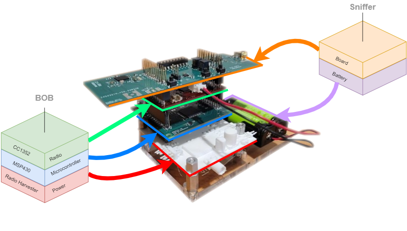
BOB
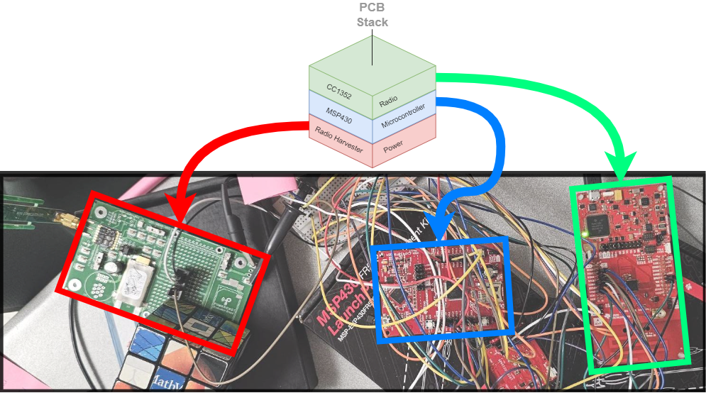 Figure 2:: BOB Stack. The top image is an abstract representation of the PCB BOB stack. The image below is a BOB the research team had wired together for testing.
The BOB is a combination of 3 PCB boards, a radio harvester board, a MSP430 microcontroller board, and a CC1352R1 radio board. In figure 1, the radio harvester board is in the red rectangle, the MSP430 microcontroller is in the blue rectangle, and the CC1352 board is in the green rectangle.
The radio harvester collects radio waves in the environment via the antenna (top left of the image) and generates electrical power to charge a capacitor. Once the capacitor is charged, the MSP430 and CC1352 boards turn on for a short period and the BOB can transmit or recieve data.
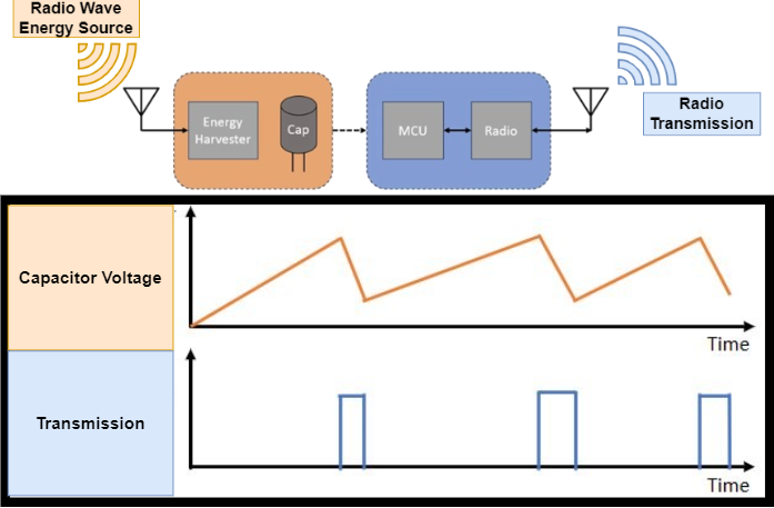
How fast the capacitor for the BOB node charges is dependent on how much radio wave energy at the harvesting frequency is available in the environment. The research team may decide to switch the batteryless power source in the future to something other than radio harvesting (such as microwind or solar), but the fundemental goal is to keep the BOB batteryless.
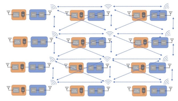
A BOB node network (shown in figure 3) allows BOBs to send and recieve data from each other. The goal of a BOB node network is to allow for the collection and transfer of data on a large scale. The wireless transmission between BOBs allows them to be spread out. Data collected by BOBs are eventually transfered to a computer system for processing. It is possible that a BOB would be out of range to send data, so having a BOB node network allows the BOB device to send its data to another BOB in range and then to the computer for processing. Data passing could involve more than just two BOBs, and there could be a system where three, four, or more BOBs could create a chain to pass data before reaching a computer system. The passing of data between BOBs allows for a larger network.
A large BOB node network can become complex. Since all the BOBs are batteryless and their power sources vary depending on the energy available in the environment, the ON/OFF times for each BOB is different. BOBs can only send data between each other if both are on at the same time. Depending on the sensors attached to the BOBs and how the BOBs are configured to send data, the data packets and there destinations can differ. All these vairations make a BOB network hard to monitor, so our job as a senior design team was to develop devices called sniffers that would monitor the BOBs ON/OFF times, the data packets the BOBs were sending, and the destination of those packets.
Sniffer
Software
- Programmed in C
- Developed in Code Composer Studio
- Built with TI-RTOS (Texas Instruments Real Time Operating System)
- Task Based Programming
Hardware
- PCBs designed in KiCad
- Researched TI designs for RF considerations
- Researched and desgned battery system to keep the sniffer boards running for a week
- Made a bill of materials for sniffer board and orderd parts
- Simulated RF S parameters for tuning
- Hand soldered and used solder oven for assembling boards
Developing the sniffer was the goal of the senior design team. The sniffer monitors the BOBs in the BOB node network to make sure they are operating as expected. They collect the ON/OFF times of the BOBs, the packets sent by the BOBs, packets received by the BOBs, and sends that data to a sink which sends data to a computer for processing. The sniffer can also configure the software on the BOBs at the beginning of a test, and simulate sensor data that BOBs would collect in a non-testing environment.
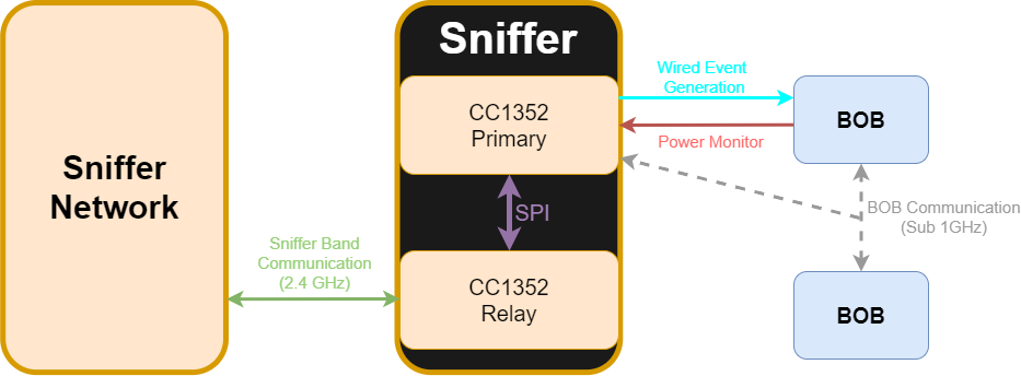
The sniffer is composed of 2 CC152 chips which we call the Primary and the Relay. The sniffer primary can send “events” to the BOB which is equivalent to the BOB recieving sensor data in a practical setting. The power monitor is a wired connection that informs the primary of the ON/OFF times of the BOB. The sub 1GHz band is how the BOBs send data between each other. The primary also collects data sent by the BOBs via the sub 1GHz band.
The sniffer primary will send the data collected from the BOB to the sniffer relay which is another CC1352 chip. The relay will send the data via a 2.4 GHz signal to either another relay on a different sniffer or to the sink depending on where the sending sniffer is located in the sniffer network (sniffer network shown in figure 7). The sending sniffer would send the data to another sniffer relay instead of the sink if the sending sniffer was out of range of the sink.

The sniffer has 4 queues (2 on the primary CC1352 chip and 2 on the relay CC1352 chip) that help to prevent data packets from being dropped. If a packet is dropped, a notification will be sent through the network to inform the user. There is one semaphore on the primary and another on the relay. In this context, the semaphores act as software “locks” that control if data can be added or removed from the queues. Queue 1 on the primary collects data sent between BOBs on the sub 1 Ghz band. Queue 2 on the primary collects the ON/OFF times of the BOB the sniffer is monitoring. Queue 1 on the relay collects data sent from the primary over SPI. Queue 2 on the relay collects data from a sniffer (or sink depending on the location of the sniffer in the network) less deep in the network, then transmits the collected data to sniffers deeper in the network. Queue 2 on the relay would be used for conifguration of the sniffers at the beginning of an experiment.
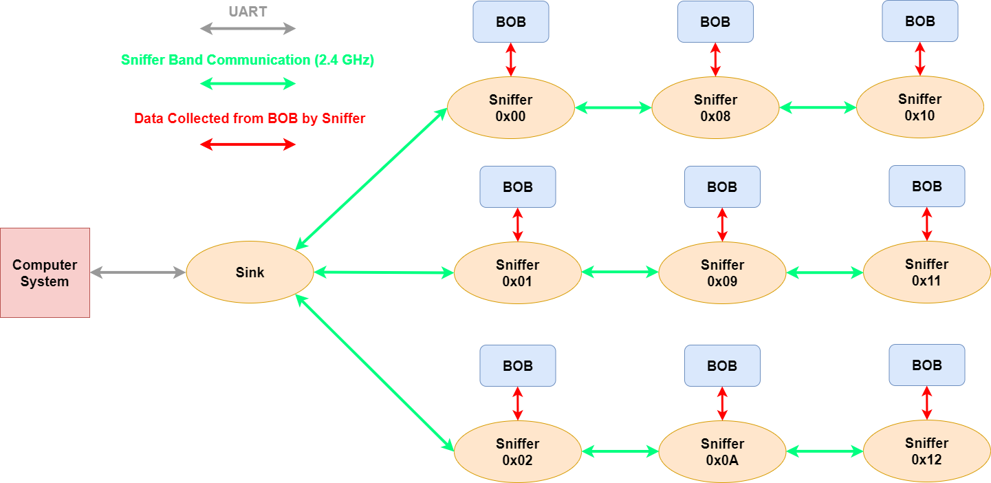
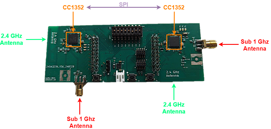
Figure 8 shows the custom sniffer produced by the senior design team. 3 sniffers were assembled before we graduated, but parts for 9 sniffers were purchased. The CC1352 chips are programmed individually and can either be the relay or the primary. The 2.4 GHz antennas are traces on the PCB, and the sub 1 GHz antenna can be screwed onto the board via the SMA connector. The switches in the center of the board were not programmed before we graduated, but we planned to use them to set the address of the sniffer which determines the location of the sniffer in the network.
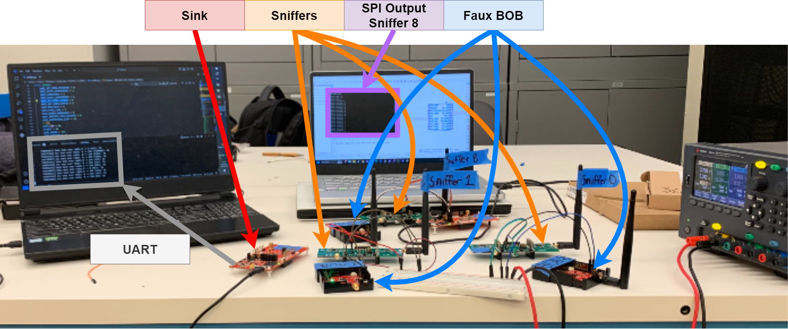
In the sniffer demo (figure 9) the sink collects data from sniffers 1 and 0 (labeled with blue tape in figure 9). Sniffer 8 sends its data to sniffer 0, which then sends both the data it collected and sniffer 8’s data to the sink. In this case, the sniffer network has a width of 2 (both sniffer 0 and 1 send to the sink) and a depth of 2 (sniffer 8 → sniffer 1 → sink). The sink sends collected data over UART to be displayed in the terminal window of the computer on the left. The terminal window on the other computer outlined in purple in figure 9 shows the data sent over SPI between the primary and relay on sniffer 8. Data is being sent over SPI on all three sniffers, but only one is shown in the figure. The Faux BOBs are programmed CC1352 chips that simulate the real BOBs. They are used to simplify the hardware needed to test the sniffers (a faux BOB requires only a single CC1352 chip compared to the real BOB which requires 3 boards (figure 2)) and to control the data the BOBs send so that we know the sniffers are operating properly.
Acknowledgements
Henry Duwe – Professor and Client. Provided guidance and answered questions for the senior design team.
Rohit Sahu – Graduate student and software lead on research team. Helped the software team solve problems throughout the project.
Vishak Narayanan – Graduate student and hardware lead on research team. Helped the hardware team with the project.
Thomas Gaul – Student and team lead for the project.
Mathew Crabb – Student and hardware developer.
Tori Kittleson – Student and hardware developer.
Spencer Sutton – Student and software developer.