Voltage Supply PCB
Project Overview
Page In Progress
I designed and assembeled a PCB in KiCad that outputs a steady 3V supply. The PCB is meant to be a test circuit for the power portion of a watch circuit I am designing (the full watch project is not currently on this website, but the final watch will have the functionality described in the IR Controller Project).
Design Constraints:
-
Output a 3V DC signal
-
Intake a variable battery voltage from 2V-5V.
-
Intake a 5V wired DC source
-
Use components previously chosen for the watch design.
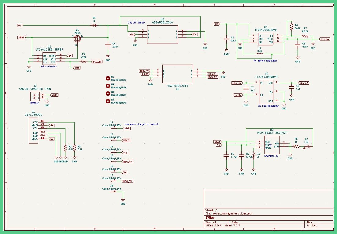
 KiCad schematic for PCB.

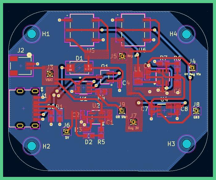
Since the design is relativly simple, the board is 2 layers. The blue/bottom layer is a ground plane, and the top layer (red) is composed of most of the other signals in the circuit.
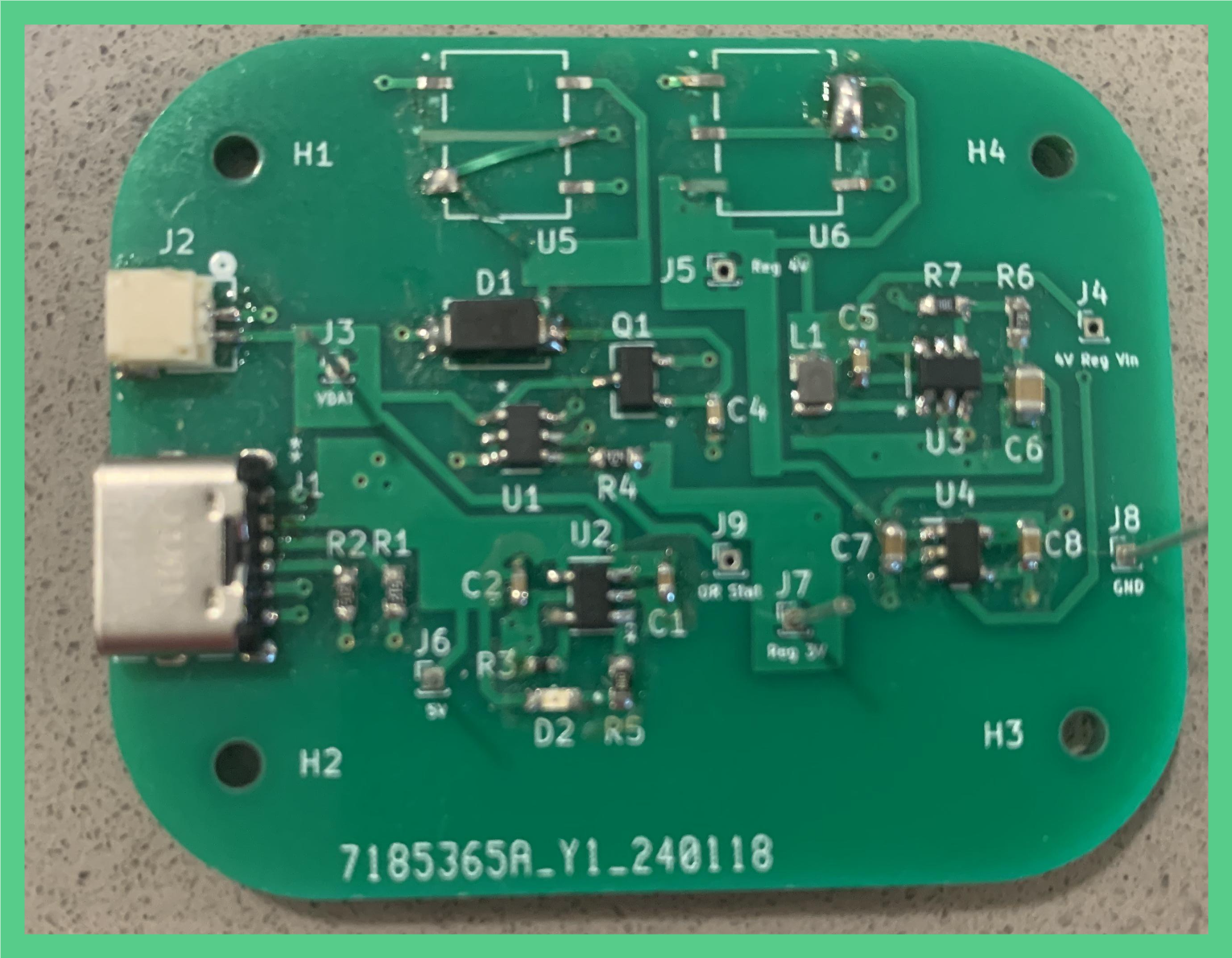
 Physical PCB
The PCD did work, but there was an issue in the switches, so I had to remove them and short the correct terminals. I bought a DPDT switch when I should have bought SPDT switch which would have been more sutiable for this application. I had issues soldering the switches onto the board, and I accidently damaged the traces remove the switch. Fortunatly I was still able to make the board work connecting the traces shown in the image above. The drawback of this connection is that the board can not be toggled ON or OFF when plugged in. One of the switches was to turn the board ON and OFF and the other was meant to enable or disable the 3V regulator.