PCB Project
Project Overview
For a class in college a partner and I designed, soldered, and tested a custom PCB. The PCB was meant to be a test board for a custom digital wrist watch. The goal was to have a programmble watch that worked with the ATmega328P microcontroller (same chip used on an Arduino). The system is designed to run on a power supply between 2.7 volts and 5 volts. The PCB supports a plug for a li-ion battery and a USB-C charging port for unboard charging of the battery. The design was a bit rushed because of the deadline constraints for school, and so the schematics are a bit messy and the PCB is not optimized for the size constriants that would be required for a wrist watch. I am currently working on this device and the IR controller project shows a more current prototype of the watch. Due to new discoveries in the IR controller project, this design is obselete but I included it on the page to show that I have worked with KiCad.
Inputs
- 4 control buttons
- Rotary Encoder (mouse scroll wheel)
- USB-C charging port
- Battery port
- IR Reciever
- ON/OFF switch
Outputs
- Buzzer
- LCD display
- IR Transmitter
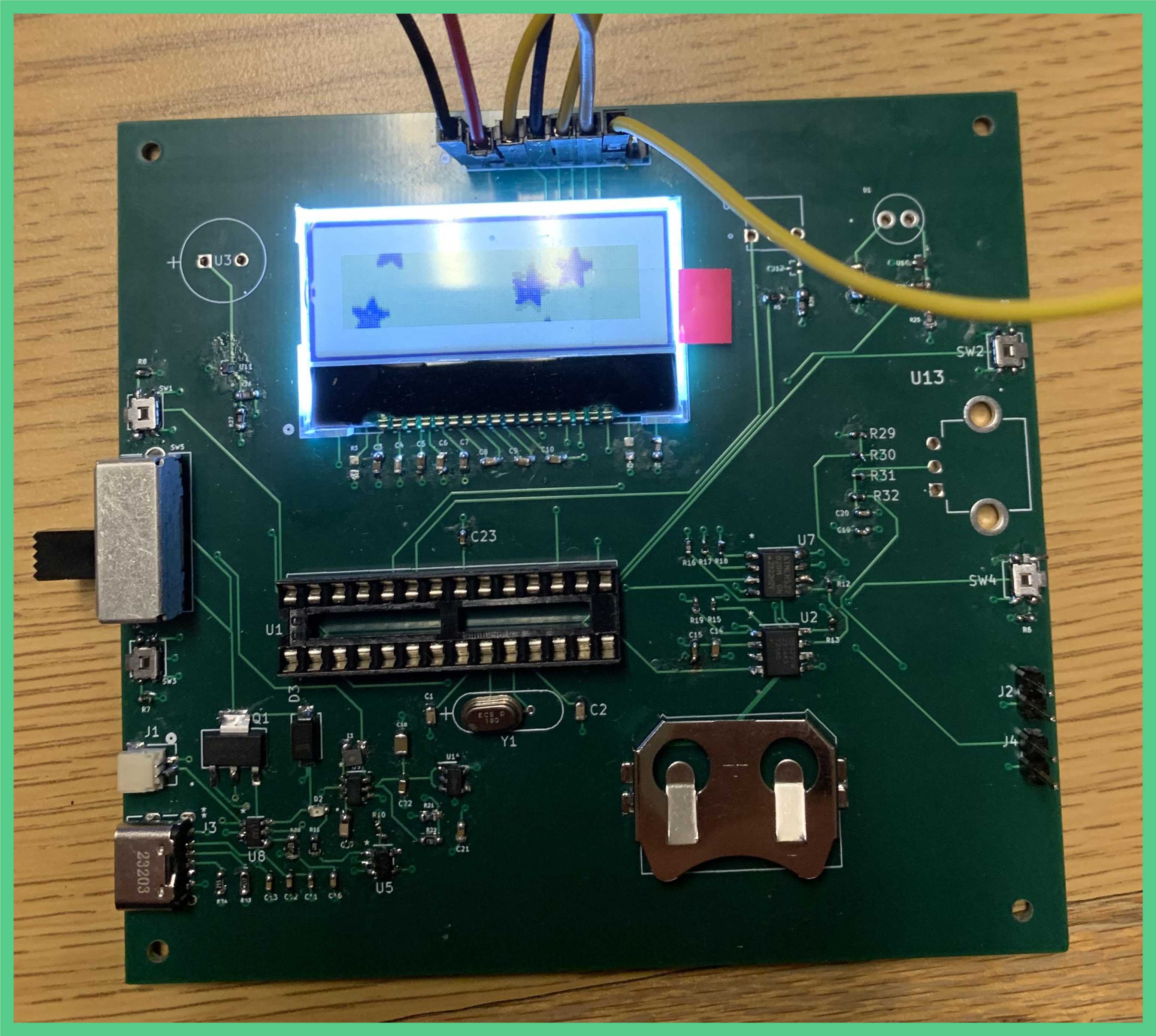 Some of the components are not soldered onto the PCB (like the buzzer, IR transmitter, IR receiver, and encoder) because they were still being tested with the Arduino. I had to make this PCB for the class, but more testing needs to be done for the watch and using breadboards is more effective than finishing this PCB, so I will not be soldering the rest of the components to the board.
Functionality
The watch includes an IR transimtter and reciever which allows the user to save and send IR signals. The watch also includes a precision clock chip to keep track of time. The precision clock chip can also be used to set alarms. On the current test board this is also a back battery to keep the precision clock chip power when the main power dies, but this my be removed from the final design because of space constraints.
Test Board 1 Design
“Test Board 1” is the first PCB designed for this project. It was made for a final project for a college course (EE333 mentioned under the education tab) and due to deadlines, this board was simplified to test basic functionality of different components in the watch, and is not intended to be the final PCB design for the wearable watch.
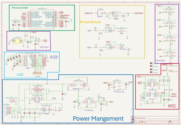
The schematic is broken down into 6 parts: microcontroller, user input, LCD, power management, RTC (real time clock) and IR and buzzer. Each sub-circuit is described in greater detail below.
Microcontroller
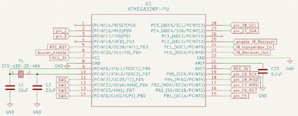
Figure 2 shows the schematic diagram for the Atmega328P microcontroller with all its connections to various parts of the circuit. Pins 1 and 2 of the microcontroller connect to the rotary encoder (dubbed the “scroll wheel” in this project). Pin 5 is the reset pin for the real time clock. Pin 6 enables the buzzer. Pin 7 is power for the chip and is connected to the 3V regulator. PIns 9 and 10 or used for the oscillator and pins 11 through 14 connect to the outputs of the pushbuttons. Pins 15 through 20 are used for the LCD screen and make use of SPI communication. Pin 23 receives the output of the IR receiver, pin 24 is IR transmitter enable, and pin 25 is IR receiver enable. Pins 28 and 27 communicate with the RTC via I2C communication.
User Input
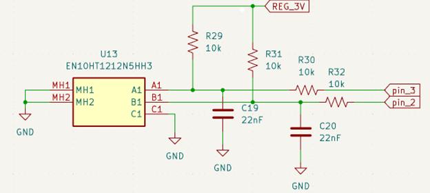
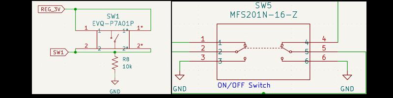
The scroll wheel is a 10 mm encoder with a 2-bit gray code. That, along with the push buttons will be the way that the users will interact with the device. Their outputs will be used to input commands into the microcontroller. The outputs of the buttons are also connected to a 10kOhm pull-down resistor to drive the button output to zero when the button is not pressed. The ON/OFF switch does not interact with the microcontroller directly. It handles the ON/OFF states of the device and it interacts with the charging part of the circuit.
LCD
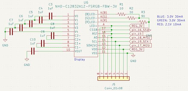
The LCD display has a 128 x 32 pixels resolution and a 5-line MPU interface that works with an ST7565R controller. It operates on a +3.0V power supply and it has a 1/33 duty cycle and 1/6 bias. It communicates with the microcontroller using SPI communication. The J5 connector was used in testing to control the LCD screen with an Arduino. The LCD screen shown in figure 5 has RGB capabilities, but our final design only has a black and white version of the same LCD screen because of mistakes made in the BOM. The footprint was similar enough so the device still works, but the K(B), K(G), and K(R) pins are unused on the PCB.
Power Mangement
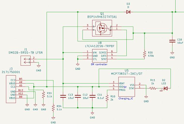
In figure 6, U8 is the OR controller which drives the gate of a P-channel MOSFET to turn ON/OFF battery power to the rest of the circuit. The OR controller was wired for automatic switching of the load between battery and continuous power based on the typical application section of the datasheet (figure 3 in the typical application section of the datasheet). In figure 6, U5 is the charging IC which charges the battery at connector J1 with the power provided at connector J3. The 2k resistor connected to the program pin of U5 sets the charging current. Page 15 of the datasheet discusses the calculation for charging current. WIth the 2k resistor the changing current for the battery is set to 0.5mA
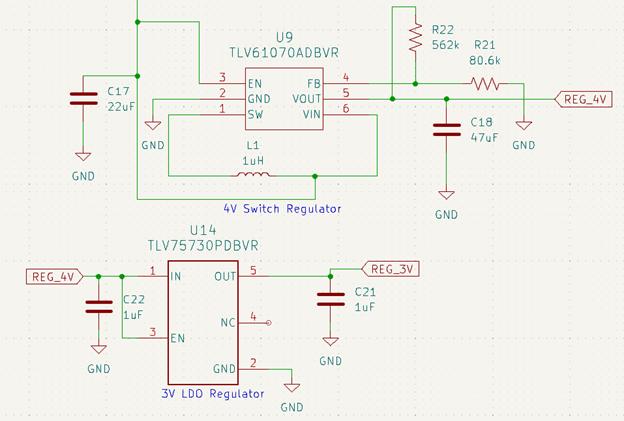
Figure 7 shows the two voltage regulators used in the circuit. The battery has a voltage that can range between 2.7V and 3.8V. Some parts of the circuit require a minimum of 3V to operate and could be damaged by voltages greater than 3.3V, so the changing voltage of the battery does not work for the system. Depending on the battery’s charge, the voltage could be too high or too low. To combat this problem, two voltage regulators were used. The first voltage regulator was a boost switching regulator to pull the voltage from the battery up to 4V. Then, a 3V LDO buck regulator was placed in series with the 4V switching regulator to drop the voltage back down to a constant 3V to operate the PCB. Our original plan was to use an IC capable of both buck and boost regulation, but we had trouble finding an IC capable of such a task with hand solderable packaging. In our project 2 meeting, Professor Tayeb suggested the series connected regulators, which we ended up using.
Real-Time Clock (RTC)
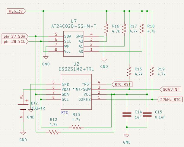
The circuit design shown is based on an Arduino module named “DS3231M RTC with EEPROM Module“ that uses the same RTC IC chip and EEPROM chip as in figure 8. “pin_27_SDA” and “pin_28_SCL” are used for I2C communication with the Atmega328P. The RTC IC chip also has an output for a 1Hz square wave and a 32kHz wave which can be seen on the right of figure 8 labeled as “SQW/INT” and “32kHz_RTC”. The 4.7kOhm pullup resistors were added based on recommendations of the datasheet.
IR and Buzzer
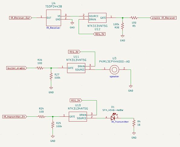
The IR receiver, IR transmitter, and buzzer are all connected to the source of an n-channel MOSFET. The drain of all the MOSFETs are connected to the output of the 3V regulator. The gates of the MOSFETs are each driven by a different pin on the Atmega328P that acts as an enable pin for each device. The gate of the MOSFETs are also connected to a 100kOhm pull-down resistor to pull the voltage of the gate to zero when the respective enable pin is off.
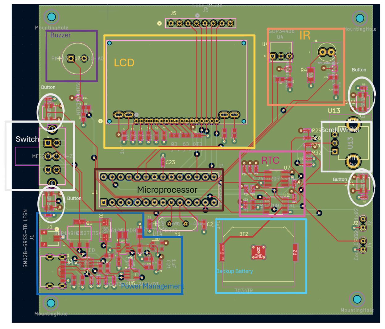
Above we have our PCB layout design from KiCAD It is a four-layer board with a ground layer, power layer and 2 layers of traces. The traces are mostly 0.25 mm in width with some that are 0.5mm. This layout is the first one made to test functionality of different components on the watch. The final PCB will be much smaller and compact.